
Xeon is a brand of x86 microprocessors designed, manufactured, and marketed by Intel, targeted at the non-consumer workstation, server, and embedded markets. It was introduced in June 1998. Xeon processors are based on the same architecture as regular desktop-grade CPUs, but have advanced features such as support for error correction code (ECC) memory, higher core counts, more PCI Express lanes, support for larger amounts of RAM, larger cache memory and extra provision for enterprise-grade reliability, availability and serviceability (RAS) features responsible for handling hardware exceptions through the Machine Check Architecture (MCA). They are often capable of safely continuing execution where a normal processor cannot due to these extra RAS features, depending on the type and severity of the machine-check exception (MCE). Some also support multi-socket systems with two, four, or eight sockets through use of the Ultra Path Interconnect (UPI) bus.

The land grid array (LGA) is a type of surface-mount packaging for integrated circuits (ICs) that is notable for having the pins on the socket — as opposed to pins on the integrated circuit, known as a pin grid array (PGA). An LGA can be electrically connected to a printed circuit board (PCB) either by the use of a socket or by soldering directly to the board.
The Intel QuickPath Interconnect (QPI) is a point-to-point processor interconnect developed by Intel which replaced the front-side bus (FSB) in Xeon, Itanium, and certain desktop platforms starting in 2008. It increased the scalability and available bandwidth. Prior to the name's announcement, Intel referred to it as Common System Interface (CSI). Earlier incarnations were known as Yet Another Protocol (YAP) and YAP+.
The Intel Core microarchitecture is a multi-core processor microarchitecture launched by Intel in mid-2006. It is a major evolution over the Yonah, the previous iteration of the P6 microarchitecture series which started in 1995 with Pentium Pro. It also replaced the NetBurst microarchitecture, which suffered from high power consumption and heat intensity due to an inefficient pipeline designed for high clock rate. In early 2004 the new version of NetBurst (Prescott) needed very high power to reach the clocks it needed for competitive performance, making it unsuitable for the shift to dual/multi-core CPUs. On May 7, 2004 Intel confirmed the cancellation of the next NetBurst, Tejas and Jayhawk. Intel had been developing Merom, the 64-bit evolution of the Pentium M, since 2001, and decided to expand it to all market segments, replacing NetBurst in desktop computers and servers. It inherited from Pentium M the choice of a short and efficient pipeline, delivering superior performance despite not reaching the high clocks of NetBurst.

Nehalem is the codename for Intel's 45 nm microarchitecture released in November 2008. It was used in the first generation of the Intel Core i5 and i7 processors, and succeeds the older Core microarchitecture used on Core 2 processors. The term "Nehalem" comes from the Nehalem River.

Sandy Bridge is the codename for Intel's 32 nm microarchitecture used in the second generation of the Intel Core processors. The Sandy Bridge microarchitecture is the successor to Nehalem and Westmere microarchitecture. Intel demonstrated an A1 stepping Sandy Bridge processor in 2009 during Intel Developer Forum (IDF), and released first products based on the architecture in January 2011 under the Core brand.

The Platform Controller Hub (PCH) is a family of Intel's single-chip chipsets, first introduced in 2009. It is the successor to the Intel Hub Architecture, which used two chips–a northbridge and southbridge, and first appeared in the Intel 5 Series.

Haswell is the codename for a processor microarchitecture developed by Intel as the "fourth-generation core" successor to the Ivy Bridge. Intel officially announced CPUs based on this microarchitecture on June 4, 2013, at Computex Taipei 2013, while a working Haswell chip was demonstrated at the 2011 Intel Developer Forum. With Haswell, which uses a 22 nm process, Intel also introduced low-power processors designed for convertible or "hybrid" ultrabooks, designated by the "U" suffix.
Bloomfield is the code name for Intel high-end desktop processors sold as Core i7-9xx and single-processor servers sold as Xeon 35xx., in almost identical configurations, replacing the earlier Yorkfield processors. The Bloomfield core is closely related to the dual-processor Gainestown, which has the same CPUID value of 0106Ax and which uses the same socket. Bloomfield uses a different socket than the later Lynnfield and Clarksfield processors based on the same 45 nm Nehalem microarchitecture, even though some of these share the same Intel Core i7 brand.

Intel Core is a line of multi-core central processing units (CPUs) for midrange, embedded, workstation and enthusiast computer markets marketed by Intel Corporation. These processors displaced the existing mid- to high-end Pentium processors at the time of their introduction, moving the Pentium to the entry level. Identical or more capable versions of Core processors are also sold as Xeon processors for the server and workstation markets.

LGA 2011, also called Socket R, is a CPU socket by Intel released on November 14, 2011. It launched along with LGA 1356 to replace its predecessor, LGA 1366 and LGA 1567. While LGA 1356 was designed for dual-processor or low-end servers, LGA 2011 was designed for high-end desktops and high-performance servers. The socket has 2011 protruding pins that touch contact points on the underside of the processor.

Skylake is Intel's codename for its sixth generation Core microprocessor family that was launched on August 5, 2015, succeeding the Broadwell microarchitecture. Skylake is a microarchitecture redesign using the same 14 nm manufacturing process technology as its predecessor, serving as a tock in Intel's tick–tock manufacturing and design model. According to Intel, the redesign brings greater CPU and GPU performance and reduced power consumption. Skylake CPUs share their microarchitecture with Kaby Lake, Coffee Lake, Whiskey Lake, and Comet Lake CPUs.

Ivy Bridge is the codename for Intel's 22 nm microarchitecture used in the third generation of the Intel Core processors. Ivy Bridge is a die shrink to 22 nm process based on FinFET ("3D") Tri-Gate transistors, from the former generation's 32 nm Sandy Bridge microarchitecture—also known as tick–tock model. The name is also applied more broadly to the Xeon and Core i7 Extreme Ivy Bridge-E series of processors released in 2013.
Intel Sandy Bridge-based Xeon microprocessors are microprocessors based on the Intel's 32 nm Sandy Bridge architecture for servers, workstations, and high-end desktops. It succeeds the six-core Gulftown/Westmere-EP processor which used the older LGA 1366 package, and uses LGA 2011, LGA 1356 and LGA 1155 socket depending on the package.

Westmere is the code name given to the 32 nm die shrink of Nehalem. While sharing the same CPU sockets, Westmere included Intel HD Graphics, while Nehalem did not.

LGA 1151, also known as Socket H4, is a type of zero insertion force flip-chip land grid array (LGA) socket for Intel desktop processors which comes in two distinct versions: the first revision which supports both Intel's Skylake and Kaby Lake CPUs, and the second revision which supports Coffee Lake CPUs exclusively.
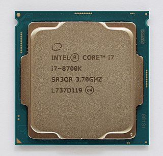
Coffee Lake is Intel's codename for its eighth-generation Core microprocessor family, announced on September 25, 2017. It is manufactured using Intel's second 14 nm process node refinement. Desktop Coffee Lake processors introduced i5 and i7 CPUs featuring six cores and Core i3 CPUs with four cores and no hyperthreading.
Raptor Lake is Intel's codename for the 13th and 14th generations of Intel Core processors based on a hybrid architecture, utilizing Raptor Cove performance cores and Gracemont efficient cores. Like Alder Lake, Raptor Lake is fabricated using Intel's Intel 7 process. Raptor Lake features up to 24 cores and 32 threads and is socket compatible with Alder Lake systems. Like earlier generations, Raptor Lake processors also need accompanying chipsets.