Local oxidation nanolithography

Last updated
Local oxidation procedure: 3D representation the Local Oxidation Nanolithography process. A voltage pulse applied between the AFM tip and the scanned surface yields to the formation of a liquid meniscus that confines a nanometric oxidation reaction. LO Matrix.PNG
Local oxidation procedure: 3D representation the Local Oxidation Nanolithography process. A voltage pulse applied between the AFM tip and the scanned surface yields to the formation of a liquid meniscus that confines a nanometric oxidation reaction.

Local oxidation nanolithography (LON) is a tip-based nanofabrication method. It is based on the spatial confinement on an oxidation reaction under the sharp tip of an atomic force microscope.

Contents

The first materials on which LON was demonstrated were Si(111) and polycrystalline tantalum. Subsequently, the technique has been extended to IIIV semiconductors, silicon carbide, metals such as titanium, tantalum, aluminium, molybdenum, nickel and niobium; thin films of manganite in the perovskite form; dielectrics like silicon nitride, organosilane self-assembled monolayers, dendritic macromolecules and carbonaceous films. [1]

History

The local oxidation of a surface by means of a scanning probe technique was first observed by Dagata and co-workers in 1990 who locally modified a hydrogen-terminated silicon surface into silicon dioxide by applying a bias voltage between the tip of a scanning tunneling microscope and the surface itself. [2] In 1993 Day and Allee demonstrated the possibility of performing local oxidation experiments with an atomic force microscope, which opened the way to applying the technique to a large variety of materials. [3]

Basic principle

Steps of the local oxidation process in noncontact mode. I: The tip is scanning the sample in noncontact mode oscillating at a constant amplitude. II:When the voltage pulse is applied a liquid meniscus between tip and sample is induced by the electrical field. This liquid meniscus acts like a nanometer-size electrochemical cell where an oxidation reaction is held. III:When the voltage pulse is off, the AFM feedbacks withdraw the tip from the sample stretching the liquid meniscus. IV: After the meniscus is broken the tip recovers its original oscillation amplitude and continues the scanning. LO steps.PNG
Steps of the local oxidation process in noncontact mode. I: The tip is scanning the sample in noncontact mode oscillating at a constant amplitude. II:When the voltage pulse is applied a liquid meniscus between tip and sample is induced by the electrical field. This liquid meniscus acts like a nanometer-size electrochemical cell where an oxidation reaction is held. III:When the voltage pulse is off, the AFM feedbacks withdraw the tip from the sample stretching the liquid meniscus. IV: After the meniscus is broken the tip recovers its original oscillation amplitude and continues the scanning.

Currently, local oxidation experiments are performed with an atomic force microscope operated in contact or noncontact mode with additional circuits to apply voltage pulses between tip and sample. The local oxidation process is mediated by the formation of a water meniscus. [4]

In order to perform local oxidation nanolithography, the relative humidity in the AFM chamber is kept between 30% and 60%. A voltage pulse is applied between a conductive AFM tip and the sample. The applied voltage induces the formation of a water bridge between tip and sample whenever the amplitude of the voltage pulse is above a certain threshold voltage. When the liquid meniscus is created the applied voltage pulse causes an oxidation reaction by breaking the covalent bonds in the water molecules. The liquid bridge provides the oxyanions (OH,O) needed to form the oxide and confines the lateral extension of the region to be oxidized.

The chemical reactions that govern the local oxidation in a metallic substrate (M) are the following: [5]

while hydrogen gas is liberated at the AFM tip through the reduction reaction:

When the voltage pulse is off the AFM feedback forces the cantilever to recover its original oscillation amplitude withdrawing the tip from the sample and breaking the liquid meniscus. Finally the AFM continues to scan the sample thus allowing to image MOn nanostructure fabricated during the Local Oxidation process with the very same tip used for its fabrication.

The method to form liquid bridges is so precise that water meniscus diameters of 20 nm or below are easily obtained. This has led to the reproducible fabrication of sub-10 nm structures in silicon and other metallic surfaces.

Experimental setup

Local oxidation experiments can be performed with almost any kind of atomic force microscope. The key requirement is the possibility to apply voltage pulses between the tip and the sample. It is recommendable to enclose the microscope in a chamber where the atmosphere is controlled. In the simplest case, the oxidant is water vapor, which is naturally present in the air. Controlling the relative humidity generally helps to obtain more reproducible results. The size of the fabricated features depends on a number of parameters, such as the distance between the sample and the tip, the amplitude and the duration of the voltage pulse, and the relative humidity of the atmosphere.

Applications

First paragraph of Cervantes' Don Quixote written on a silicon chip. The local oxidation technique would allow to write all the book (more than 1,000 pages) on a surface as big as the tip of one human hair. QuijoteFinal.JPG
First paragraph of Cervantes' Don Quixote written on a silicon chip. The local oxidation technique would allow to write all the book (more than 1,000 pages) on a surface as big as the tip of one human hair.

The development of nanometer-scale lithographies is the focus of an intense research activity because progress on nanotechnology depends on the capability to fabricate, position and interconnect nanometer-scale structures.

Patterning

Local Oxidation Nanolithography allows to create a large variety of motives like dots, lines and letters with nanometer accuracy. In 2005, researchers at the Spanish National Research Council in Madrid wrote the first ten lines of Cervantes' Don Quixote on a few square micrometres of silicon. [1] This pattern versatility can be used for information storage or to design etch-resistant nanomasks in order to fabricate nanodevices as well as many other applications.

Data storage

p number with twenty decimals: 3,1415926535 8979323846 written in binary code by Local Oxidation on a silicon surface. PI-number-LON.png
π number with twenty decimals: 3,1415926535 8979323846 written in binary code by Local Oxidation on a silicon surface.

It is possible to store information using dot-like nanostructures created by the local oxidation of a surface. This storage uses the binary code considering the presence of a nanostructure as a 1 and its lack as a 0. In this way information can be stored in a small surface with a single SiO2 dot constituting a bit. In 1999 Cooper et al. demonstrated that this methods allows to obtain an information density of 1.6 Tbit/in2. [6] However, only read-only memories can be fabricated with this technique.

Molecular template growth and preferential deposition

Using specific functionalizations it is possible to deposit molecules and nanoparticles only in very small domains over a substrate surface. LON is a powerful technique to fabricate this kind of domains for the preferential growth. Mn12 Deposition Procedure.png
Using specific functionalizations it is possible to deposit molecules and nanoparticles only in very small domains over a substrate surface. LON is a powerful technique to fabricate this kind of domains for the preferential growth.
Two SiO2 stripes were fabricated by LON over a substrate functionalized with APTES. After the deposition of a 0.1mM solution of Mn12 the single-molecule magnets are deposited only over the regions defined by the AFM. Mn12 before and after.png
Two SiO2 stripes were fabricated by LON over a substrate functionalized with APTES. After the deposition of a 0.1mM solution of Mn12 the single-molecule magnets are deposited only over the regions defined by the AFM.

Local oxidation of silicon surfaces by noncontact atomic-force microscopy is an emerging and promising method for patterning surfaces at the nanometer scale due to its very precise control of the feature size. The features created with this technique can be used for the template growth and preferential deposition of different molecules like single-molecule magnets, biomolecules and conjugated organic molecules. This method of nanopositioning is an important tool for the fabrication of new nanodevices based on the novel properties exhibited by some nanoparticles and molecules. Potential applications of single-molecule magnets (SMMs) such as Mn12 as bits for information storage or qubits for quantum computation require methods for nanoscale-controlled positioning and/or manipulation of those molecules. [7] The patterning of the Mn12 molecules on a silicon surface is achieved by first derivatizing this surface with a self-assembled monolayer of APTES, which leaves it terminated by amino groups (-NH2). Such termination electrostatically repels the Mn12 molecules. Subsequently, a pattern of silicon dioxide is defined by LON. The SMM molecules are predominantly deposited on the oxide motives because of electrostatic attraction. The electrostatic attraction between the silicon oxide fabricated by LON and the Mn12 molecules achieves the preferential deposition of this molecules with a nanoscale accuracy.

Fabrication of nanodevices

In order to fabricate SiNW using the Top-Down approach of the nanotechnology a nanomask is fabricated by LON over a Silicon On Insulator substrate. After the SOI etching a SiNW is defined under the nanomask. Then the nanomask is removed with a HF etching and finally the SiNW is connected to the whole circuit using Electron Beam lithography. SiNW Fabrication.png
In order to fabricate SiNW using the Top-Down approach of the nanotechnology a nanomask is fabricated by LON over a Silicon On Insulator substrate. After the SOI etching a SiNW is defined under the nanomask. Then the nanomask is removed with a HF etching and finally the SiNW is connected to the whole circuit using Electron Beam lithography.
SiNW nanotransistor fabricated with the term 'NANO'. This pattern exhibits a good electrical response based on in the SiNW properties only. Silicon nanowire transistor in the shape of the word NANO.jpg
SiNW nanotransistor fabricated with the term 'NANO'. This pattern exhibits a good electrical response based on in the SiNW properties only.

By using local oxidation nanolithography as tool for the fabrication of etch-resistant nanomasks, it is possible to fabricate nanoscale electronic devices, such as field-effect transistors, single-electron transistors, Josephson junctions, quantum rings or SQUIDs. [5] LON also allows to fabricate silicon nanowires (SiNWs) in a top-down fashion starting from silicon on insulator (SOI) wafers. [8] Local oxidation nanolithography contributes to the nanometric precision of the device fabrication. This top-down fabrication technique allows the fabrication of a large variety of SiNWs with different shapes, from angular to circular. It also allows the precise positioning of the silicon nanowires in any desired position, making easier its integration; indeed, this technique is compatible with the standard silicon CMOS processing technology. Single crystalline silicon nanowires have already shown a great potential as ultrasensitive sensors by detecting changes in the nanowire conductivity when a specific analyte is present. [9] Local oxidation nanolithography, therefore, is a promising technique to allow the realisation of array of biosensors.

Related Research Articles

<span class="mw-page-title-main">Nanotechnology</span> Field of science involving control of matter on atomic and (supra)molecular scales

Nanotechnology was defined by the National Nanotechnology Initiative as the manipulation of matter with at least one dimension sized from 1 to 100 nanometers (nm). At this scale, commonly known as the nanoscale, surface area and quantum mechanical effects become important in describing properties of matter. The definition of nanotechnology is inclusive of all types of research and technologies that deal with these special properties. It is therefore common to see the plural form "nanotechnologies" as well as "nanoscale technologies" to refer to the broad range of research and applications whose common trait is size. An earlier description of nanotechnology referred to the particular technological goal of precisely manipulating atoms and molecules for fabrication of macroscale products, also now referred to as molecular nanotechnology.

A nanowire is a nanostructure in the form of a wire with the diameter of the order of a nanometre. More generally, nanowires can be defined as structures that have a thickness or diameter constrained to tens of nanometers or less and an unconstrained length. At these scales, quantum mechanical effects are important—which coined the term "quantum wires".

<span class="mw-page-title-main">Atomic force microscopy</span> Type of microscopy

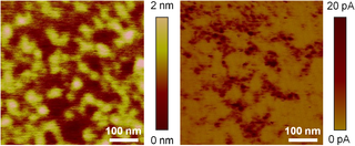
Atomic force microscopy (AFM) or scanning force microscopy (SFM) is a very-high-resolution type of scanning probe microscopy (SPM), with demonstrated resolution on the order of fractions of a nanometer, more than 1000 times better than the optical diffraction limit.

Scanning probe microscopy (SPM) is a branch of microscopy that forms images of surfaces using a physical probe that scans the specimen. SPM was founded in 1981, with the invention of the scanning tunneling microscope, an instrument for imaging surfaces at the atomic level. The first successful scanning tunneling microscope experiment was done by Gerd Binnig and Heinrich Rohrer. The key to their success was using a feedback loop to regulate gap distance between the sample and the probe.

<span class="mw-page-title-main">Dip-pen nanolithography</span> Scanning probe lithographic technique

Dip pen nanolithography (DPN) is a scanning probe lithography technique where an atomic force microscope (AFM) tip is used to create patterns directly on a range of substances with a variety of inks. A common example of this technique is exemplified by the use of alkane thiolates to imprint onto a gold surface. This technique allows surface patterning on scales of under 100 nanometers. DPN is the nanotechnology analog of the dip pen, where the tip of an atomic force microscope cantilever acts as a "pen", which is coated with a chemical compound or mixture acting as an "ink", and put in contact with a substrate, the "paper".

<span class="mw-page-title-main">Magnetic force microscope</span>

Magnetic force microscopy (MFM) is a variety of atomic force microscopy, in which a sharp magnetized tip scans a magnetic sample; the tip-sample magnetic interactions are detected and used to reconstruct the magnetic structure of the sample surface. Many kinds of magnetic interactions are measured by MFM, including magnetic dipole–dipole interaction. MFM scanning often uses non-contact AFM (NC-AFM) mode.

Electrostatic force microscopy (EFM) is a type of dynamic non-contact atomic force microscopy where the electrostatic force is probed.. This force arises due to the attraction or repulsion of separated charges. It is a long-range force and can be detected 100 nm or more from the sample.

Scanning probe lithography (SPL) describes a set of nanolithographic methods to pattern material on the nanoscale using scanning probes. It is a direct-write, mask-less approach which bypasses the diffraction limit and can reach resolutions below 10 nm. It is considered an alternative lithographic technology often used in academic and research environments. The term scanning probe lithography was coined after the first patterning experiments with scanning probe microscopes (SPM) in the late 1980s.

<span class="mw-page-title-main">Nanometrology</span> Metrology of nanomaterials

Nanometrology is a subfield of metrology, concerned with the science of measurement at the nanoscale level. Nanometrology has a crucial role in order to produce nanomaterials and devices with a high degree of accuracy and reliability in nanomanufacturing.

<span class="mw-page-title-main">Conductive atomic force microscopy</span> Method of measuring the microscopic topography of a material

In microscopy, conductive atomic force microscopy (C-AFM) or current sensing atomic force microscopy (CS-AFM) is a mode in atomic force microscopy (AFM) that simultaneously measures the topography of a material and the electric current flow at the contact point of the tip with the surface of the sample. The topography is measured by detecting the deflection of the cantilever using an optical system, while the current is detected using a current-to-voltage preamplifier. The fact that the CAFM uses two different detection systems is a strong advantage compared to scanning tunneling microscopy (STM). Basically, in STM the topography picture is constructed based on the current flowing between the tip and the sample. Therefore, when a portion of a sample is scanned with an STM, it is not possible to discern if the current fluctuations are related to a change in the topography or to a change in the sample conductivity.

<span class="mw-page-title-main">Piezoresponse force microscopy</span> Microscopy technique for piezoelectric materials

Piezoresponse force microscopy (PFM) is a variant of atomic force microscopy (AFM) that allows imaging and manipulation of piezoelectric/ferroelectric materials domains. This is achieved by bringing a sharp conductive probe into contact with a ferroelectric surface and applying an alternating current (AC) bias to the probe tip in order to excite deformation of the sample through the converse piezoelectric effect (CPE). The resulting deflection of the probe cantilever is detected through standard split photodiode detector methods and then demodulated by use of a lock-in amplifier (LiA). In this way topography and ferroelectric domains can be imaged simultaneously with high resolution.

<span class="mw-page-title-main">Thermal scanning probe lithography</span>

Thermal scanning probe lithography (t-SPL) is a form of scanning probe lithography (SPL) whereby material is structured on the nanoscale using scanning probes, primarily through the application of thermal energy.

<span class="mw-page-title-main">Photoconductive atomic force microscopy</span> Type of atomic force microscopy

Photoconductive atomic force microscopy (PC-AFM) is a variant of atomic force microscopy that measures photoconductivity in addition to surface forces.

The technique of vibrational analysis with scanning probe microscopy allows probing vibrational properties of materials at the submicrometer scale, and even of individual molecules. This is accomplished by integrating scanning probe microscopy (SPM) and vibrational spectroscopy. This combination allows for much higher spatial resolution than can be achieved with conventional Raman/FTIR instrumentation. The technique is also nondestructive, requires non-extensive sample preparation, and provides more contrast such as intensity contrast, polarization contrast and wavelength contrast, as well as providing specific chemical information and topography images simultaneously.

Thermochemical nanolithography (TCNL) or thermochemical scanning probe lithography (tc-SPL) is a scanning probe microscopy-based nanolithography technique which triggers thermally activated chemical reactions to change the chemical functionality or the phase of surfaces. Chemical changes can be written very quickly through rapid probe scanning, since no mass is transferred from the tip to the surface, and writing speed is limited only by the heat transfer rate. TCNL was invented in 2007 by a group at the Georgia Institute of Technology. Riedo and collaborators demonstrated that TCNL can produce local chemical changes with feature sizes down to 12 nm at scan speeds up to 1 mm/s.

<span class="mw-page-title-main">Non-contact atomic force microscopy</span>

Non-contact atomic force microscopy (nc-AFM), also known as dynamic force microscopy (DFM), is a mode of atomic force microscopy, which itself is a type of scanning probe microscopy. In nc-AFM a sharp probe is moved close to the surface under study, the probe is then raster scanned across the surface, the image is then constructed from the force interactions during the scan. The probe is connected to a resonator, usually a silicon cantilever or a quartz crystal resonator. During measurements the sensor is driven so that it oscillates. The force interactions are measured either by measuring the change in amplitude of the oscillation at a constant frequency just off resonance or by measuring the change in resonant frequency directly using a feedback circuit to always drive the sensor on resonance.

A probe tip is an instrument used in scanning probe microscopes (SPMs) to scan the surface of a sample and make nano-scale images of surfaces and structures. The probe tip is mounted on the end of a cantilever and can be as sharp as a single atom. In microscopy, probe tip geometry and the composition of both the tip and the surface being probed directly affect resolution and imaging quality. Tip size and shape are extremely important in monitoring and detecting interactions between surfaces. SPMs can precisely measure electrostatic forces, magnetic forces, chemical bonding, Van der Waals forces, and capillary forces. SPMs can also reveal the morphology and topography of a surface.

Electrochemical AFM (EC-AFM) is a particular type of Scanning probe microscopy (SPM), which combines the classical Atomic force microscopy (AFM) together with electrochemical measurements. EC-AFM allows to perform in-situ AFM measurements in an electrochemical cell, in order to investigate the actual changes in the electrode surface morphology during electrochemical reactions. The solid-liquid interface is thus investigated. This technique was developed for the first time in 1996 by Kouzeki et al., who studied amorphous and polycrystalline thin films of Naphthalocyanine on Indium tin oxide in a solution of 0.1 M Potassium chloride (KCl). Unlike the Electrochemical scanning tunneling microscope, previously developed by Itaya and Tomita in 1988, the tip is non-conductive and it is easily steered in a liquid environment.

<span class="mw-page-title-main">Multi-tip scanning tunneling microscopy</span>

Multi-tip scanning tunneling microscopy extends scanning tunneling microscopy (STM) from imaging to dedicated electrical measurements at the nanoscale like a ″multimeter at the nanoscale″. In materials science, nanoscience, and nanotechnology, it is desirable to measure electrical properties at a particular position of the sample. For this purpose, multi-tip STMs in which several tips are operated independently have been developed. Apart from imaging the sample, the tips of a multi-tip STM are used to form contacts to the sample at desired locations and to perform local electrical measurements.

This glossary of nanotechnology is a list of definitions of terms and concepts relevant to nanotechnology, its sub-disciplines, and related fields.

References

  1. 1 2 Garcia, R; Martinez, RV; Martinez, J (2005). "Nano-chemistry and scanning probe nanolithographies" (PDF). Chem. Soc. Rev. 35 (1): 29–38. doi:10.1039/b501599p. PMID   16365640.
  2. Dagata, JA; Schneir, J; Harary, HH; Evans, CJ; Postek, MT; Bennett, J (1990). "Modification of hydrogen-passivated silicon by a scanning tunneling microscope operating in air". Appl. Phys. Lett. 56 (20): 2001. Bibcode:1990ApPhL..56.2001D. doi:10.1063/1.102999.
  3. Day, HC; Allee, DR (1993). "Selective area oxidation of silicon with a scanning force microscope". Appl. Phys. Lett. 62 (21): 2691. Bibcode:1993ApPhL..62.2691D. doi:10.1063/1.109259.
  4. Garcia, R; Calleja, M; Rohrer, H (1999). "Patterning of silicon surfaces with noncontact atomic force microscopy: Field-induced formation of nanometer-size water bridges" (PDF). J. Appl. Phys. 86 (4): 1898. Bibcode:1999JAP....86.1898G. doi:10.1063/1.370985. hdl: 10261/22353 .
  5. 1 2 Tello, Marta; García, Fernando; García, Ricardo (2004). Bhushan, Bharat; Fuchs, Harald (eds.). Applied Scanning Probe Methods IV – Industrial Applications . Berlin: Springer. pp.  137–158. ISBN   3-540-26912-6.
  6. Cooper, EB; Manalis, SR; Fang, H; Dai, H; Matsumoto, K (1999). "Terabit-per-square-inch data storage with the atomic force microscope". Appl. Phys. Lett. 75 (22): 3566. Bibcode:1999ApPhL..75.3566C. doi:10.1063/1.125390.
  7. Coronado, E; Epstein, AJ (2009). "Molecular spintronics and quantum computing". J. Mater. Chem. 19 (12): 1670–1671. doi:10.1039/b901955n.
  8. Martinez, J; Martínez, RV; Garcia, R (2008). "Silicon Nanowire Transistors with a Channel Width of 4 nm Fabricated by Atomic Force Microscope Nanolithography". Nano Lett. 8 (11): 3636–3639. Bibcode:2008NanoL...8.3636M. doi:10.1021/nl801599k. PMID   18826289.
  9. Cui, Y; Wei, Q; Park, H; Lieber, CM (1999). "Nanowire Nanosensors for Highly Sensitive and Selective Detection of Biological and Chemical Species". Science . 293 (5533): 1289–92. Bibcode:2001Sci...293.1289C. doi:10.1126/science.1062711. PMID   11509722.