Microphotonics is a branch of technology that deals with directing light on a microscopic scale and is used in optical networking. Particularly, it refers to the branch of technology that deals with wafer-level integrated devices and systems that emit, transmit, detect, and process light along with other forms of radiant energy with photon as the quantum unit.
Electro–optics is a branch of electrical engineering, electronic engineering, materials science, and material physics involving components, electronic devices such as lasers, laser diodes, LEDs, waveguides, etc. which operate by the propagation and interaction of light with various tailored materials. It is closely related to photonics, the branch of optics that involves the application of the generation of photons. It is not only concerned with the "electro–optic effect", since it deals with the interaction between the electromagnetic and the electrical states of materials.

Photonics is a branch of optics that involves the application of generation, detection, and manipulation of light in the form of photons through emission, transmission, modulation, signal processing, switching, amplification, and sensing.
Optics is the branch of physics which involves the behavior and properties of light, including its interactions with matter and the construction of instruments that use or detect it. Optics usually describes the behavior of visible, ultraviolet, and infrared light. Because light is an electromagnetic wave, other forms of electromagnetic radiation such as X-rays, microwaves, and radio waves exhibit similar properties.

A photonic crystal is an optical nanostructure in which the refractive index changes periodically. This affects the propagation of light in the same way that the structure of natural crystals gives rise to X-ray diffraction and that the atomic lattices of semiconductors affect their conductivity of electrons. Photonic crystals occur in nature in the form of structural coloration and animal reflectors, and, as artificially produced, promise to be useful in a range of applications.
The term biophotonics denotes a combination of biology and photonics, with photonics being the science and technology of generation, manipulation, and detection of photons, quantum units of light. Photonics is related to electronics and photons. Photons play a central role in information technologies, such as fiber optics, the way electrons do in electronics.

Photonic-crystal fiber (PCF) is a class of optical fiber based on the properties of photonic crystals. It was first explored in 1996 at University of Bath, UK. Because of its ability to confine light in hollow cores or with confinement characteristics not possible in conventional optical fiber, PCF is now finding applications in fiber-optic communications, fiber lasers, nonlinear devices, high-power transmission, highly sensitive gas sensors, and other areas. More specific categories of PCF include photonic-bandgap fiber, holey fiber, hole-assisted fiber, and Bragg fiber. Photonic crystal fibers may be considered a subgroup of a more general class of microstructured optical fibers, where light is guided by structural modifications, and not only by refractive index differences. Hollow-core fibers (HCFs) are a related type of optical fiber which bears some resemblance to holey optical fiber, but may or may not be photonic depending on the fiber.
In optics, an ARROW is a type of waveguide that uses the principle of thin-film interference to guide light with low loss. It is formed from an anti-resonant Fabry–Pérot reflector. The optical mode is leaky, but relatively low-loss propagation can be achieved by making the Fabry–Pérot reflector of sufficiently high quality or small size.

A distributed Bragg reflector (DBR) is a reflector used in waveguides, such as optical fibers. It is a structure formed from multiple layers of alternating materials with different refractive index, or by periodic variation of some characteristic of a dielectric waveguide, resulting in periodic variation in the effective refractive index in the guide. Each layer boundary causes a partial reflection and refraction of an optical wave. For waves whose vacuum wavelength is close to four times the optical thickness of the layers, the interaction between these beams generates constructive interference, and the layers act as a high-quality reflector. The range of wavelengths that are reflected is called the photonic stopband. Within this range of wavelengths, light is "forbidden" to propagate in the structure.

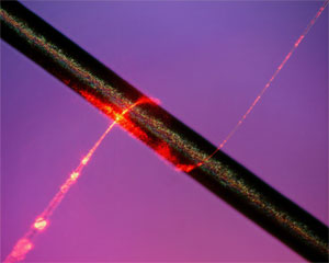
An optical fiber, or optical fibre, is a flexible glass or plastic fiber that can transmit light from one end to the other. Such fibers find wide usage in fiber-optic communications, where they permit transmission over longer distances and at higher bandwidths than electrical cables. Fibers are used instead of metal wires because signals travel along them with less loss and are immune to electromagnetic interference. Fibers are also used for illumination and imaging, and are often wrapped in bundles so they may be used to carry light into, or images out of confined spaces, as in the case of a fiberscope. Specially designed fibers are also used for a variety of other applications, such as fiber optic sensors and fiber lasers.
An optical waveguide is a physical structure that guides electromagnetic waves in the optical spectrum. Common types of optical waveguides include optical fiber waveguides, transparent dielectric waveguides made of plastic and glass, liquid light guides, and liquid waveguides.
A photonic integrated circuit (PIC) or integrated optical circuit is a microchip containing two or more photonic components that form a functioning circuit. This technology detects, generates, transports, and processes light. Photonic integrated circuits use photons as opposed to electrons that are used by electronic integrated circuits. The major difference between the two is that a photonic integrated circuit provides functions for information signals imposed on optical wavelengths typically in the visible spectrum or near-infrared (850–1650 nm).

Silicon photonics is the study and application of photonic systems which use silicon as an optical medium. The silicon is usually patterned with sub-micrometre precision, into microphotonic components. These operate in the infrared, most commonly at the 1.55 micrometre wavelength used by most fiber optic telecommunication systems. The silicon typically lies on top of a layer of silica in what is known as silicon on insulator (SOI).

Digital planar holography (DPH) is a method for designing and fabricating miniature components for integrated optics. It was invented by Vladimir Yankov and first published in 2003. The essence of the DPH technology is embedding computer designed digital holograms inside a planar waveguide. Light propagates through the plane of the hologram instead of perpendicularly, allowing for a long interaction path. Benefits of a long interaction path have long been used by volume or thick holograms. Planar configuration of the hologram provider for easier access to the embedded diagram aiding in its manufacture.

A slot-waveguide is an optical waveguide that guides strongly confined light in a subwavelength-scale low refractive index region by total internal reflection.
A subwavelength-diameter optical fibre is an optical fibre whose diameter is less than the wavelength of the light being propagated through it. An SDF usually consists of long thick parts at both ends, transition regions (tapers) where the fibre diameter gradually decreases down to the subwavelength value, and a subwavelength-diameter waist, which is the main acting part. Due to such a strong geometrical confinement, the guided electromagnetic field in an SDF is restricted to a single mode called fundamental. In usual optical fibres, light both excites and feels shear and longitudinal bulk elastic waves, giving rise to forward-guided acoustic wave Brillouin scattering and backward-stimulated Brillouin scattering. In a subwavelength-diameter optical fibre, the situation changes dramatically.
A liquid-crystal laser is a laser that uses a liquid crystal as the resonator cavity, allowing selection of emission wavelength and polarization from the active laser medium. The lasing medium is usually a dye doped into the liquid crystal. Liquid-crystal lasers are comparable in size to diode lasers, but provide the continuous wide spectrum tunability of dye lasers while maintaining a large coherence area. The tuning range is typically several tens of nanometers. Self-organization at micrometer scales reduces manufacturing complexity compared to using layered photonic metamaterials. Operation may be either in continuous wave mode or in pulsed mode.
Microstructured optical fibers (MOF) are optical fiber waveguides where guiding is obtained through manipulation of waveguide structure rather than its index of refraction.
An erbium-doped waveguide amplifier is a type of an optical amplifier enhanced with erbium. It is a close relative of an EDFA, erbium-doped fiber amplifier, and in fact EDWA's basic operating principles are identical to those of the EDFA. Both of them can be used to amplify infrared light at wavelengths in optical communication bands between 1500 and 1600 nm. However, whereas an EDFA is made using a free-standing fiber, an EDWA is typically produced on a planar substrate, sometimes in ways that are very similar to the methods used in electronic integrated circuit manufacturing. Therefore, the main advantage of EDWAs over EDFAs lies in their potential to be intimately integrated with other optical components on the same planar substrate and thus making EDFAs unnecessary.

Prof. R K Sinha is the Vice Chancellor of Gautam Buddha University, Greater Noida, Gautam Budh Nagar under Uttar Pradesh Government since January 2022. He was the Director of the CSIR-Central Scientific Instruments Organisation (CSIR-CSIO) Sector-30C, Chandigarh-160 030, India. He has been a Professor - Applied Physics, Dean-Academic [UG] & Chief Coordinator: TIFAC-Center of Relevance and Excellence in Fiber Optics and Optical Communication, Mission REACH Program, Technology Vision-2020, Govt. of India Delhi Technological University Bawana Road, Delhi-110042, India.