Features
The following table shows features of AMD's processors with 3D graphics, including APUs (see also: List of AMD processors with 3D graphics).
| Platform | High, standard and low power | Low and ultra-low power | |||||||||||||||||||||||||||||||||||||||||||||||||||||||||||||||||||||||||||||||||||||||||||||||||||
|---|---|---|---|---|---|---|---|---|---|---|---|---|---|---|---|---|---|---|---|---|---|---|---|---|---|---|---|---|---|---|---|---|---|---|---|---|---|---|---|---|---|---|---|---|---|---|---|---|---|---|---|---|---|---|---|---|---|---|---|---|---|---|---|---|---|---|---|---|---|---|---|---|---|---|---|---|---|---|---|---|---|---|---|---|---|---|---|---|---|---|---|---|---|---|---|---|---|---|---|---|---|
| Codename | Server | Basic | Toronto | ||||||||||||||||||||||||||||||||||||||||||||||||||||||||||||||||||||||||||||||||||||||||||||||||||
| Micro | Kyoto | ||||||||||||||||||||||||||||||||||||||||||||||||||||||||||||||||||||||||||||||||||||||||||||||||||||
| Desktop | Performance | Raphael | Phoenix | ||||||||||||||||||||||||||||||||||||||||||||||||||||||||||||||||||||||||||||||||||||||||||||||||||
| Mainstream | Llano | Trinity | Richland | Kaveri | Kaveri Refresh (Godavari) | Carrizo | Bristol Ridge | Raven Ridge | Picasso | Renoir | Cezanne | ||||||||||||||||||||||||||||||||||||||||||||||||||||||||||||||||||||||||||||||||||||||||||
| Entry | |||||||||||||||||||||||||||||||||||||||||||||||||||||||||||||||||||||||||||||||||||||||||||||||||||||
| Basic | Kabini | Dalí | |||||||||||||||||||||||||||||||||||||||||||||||||||||||||||||||||||||||||||||||||||||||||||||||||||
| Mobile | Performance | Renoir | Cezanne | Rembrandt | Dragon Range | ||||||||||||||||||||||||||||||||||||||||||||||||||||||||||||||||||||||||||||||||||||||||||||||||
| Mainstream | Llano | Trinity | Richland | Kaveri | Carrizo | Bristol Ridge | Raven Ridge | Picasso | Renoir Lucienne | Cezanne Barceló | Phoenix | ||||||||||||||||||||||||||||||||||||||||||||||||||||||||||||||||||||||||||||||||||||||||||
| Entry | Dalí | Mendocino | |||||||||||||||||||||||||||||||||||||||||||||||||||||||||||||||||||||||||||||||||||||||||||||||||||
| Basic | Desna, Ontario, Zacate | Kabini, Temash | Beema, Mullins | Carrizo-L | Stoney Ridge | Pollock | |||||||||||||||||||||||||||||||||||||||||||||||||||||||||||||||||||||||||||||||||||||||||||||||
| Embedded | Trinity | Bald Eagle | Merlin Falcon, Brown Falcon | Great Horned Owl | Grey Hawk | Ontario, Zacate | Kabini | Steppe Eagle, Crowned Eagle, LX-Family | Prairie Falcon | Banded Kestrel | River Hawk | ||||||||||||||||||||||||||||||||||||||||||||||||||||||||||||||||||||||||||||||||||||||||||
| Released | Aug 2011 | Oct 2012 | Jun 2013 | Jan 2014 | 2015 | Jun 2015 | Jun 2016 | Oct 2017 | Jan 2019 | Mar 2020 | Jan 2021 | Jan 2022 | Sep 2022 | Jan 2023 | Jan 2011 | May 2013 | Apr 2014 | May 2015 | Feb 2016 | Apr 2019 | Jul 2020 | Jun 2022 | Nov 2022 | ||||||||||||||||||||||||||||||||||||||||||||||||||||||||||||||||||||||||||||||
| CPU microarchitecture | K10 | Piledriver | Steamroller | Excavator | "Excavator+" [13] | Zen | Zen+ | Zen 2 | Zen 3 | Zen 3+ | Zen 4 | Bobcat | Jaguar | Puma | Puma+ [14] | "Excavator+" | Zen | Zen+ | "Zen 2+" | ||||||||||||||||||||||||||||||||||||||||||||||||||||||||||||||||||||||||||||||||||
| ISA | x86-64 v1 | x86-64 v2 | x86-64 v3 | x86-64 v4 | x86-64 v1 | x86-64 v2 | x86-64 v3 | ||||||||||||||||||||||||||||||||||||||||||||||||||||||||||||||||||||||||||||||||||||||||||||||
| Socket | Desktop | Performance | — | AM5 | — | — | |||||||||||||||||||||||||||||||||||||||||||||||||||||||||||||||||||||||||||||||||||||||||||||||
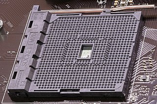
| Mainstream | — | AM4 | — | — | |||||||||||||||||||||||||||||||||||||||||||||||||||||||||||||||||||||||||||||||||||||||||||||||||
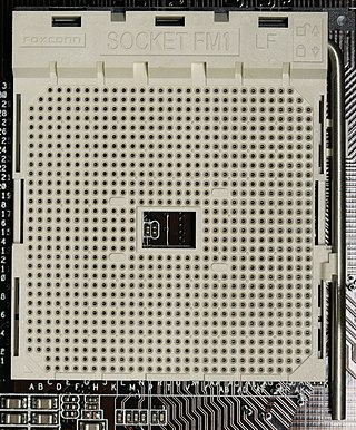
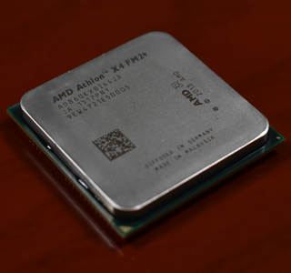
| Entry | FM1 | FM2 | FM2+ | FM2+ [lower-alpha 1] , AM4 | AM4 | — | |||||||||||||||||||||||||||||||||||||||||||||||||||||||||||||||||||||||||||||||||||||||||||||||
| Basic | — | — | AM1 | — | FP5 | — | |||||||||||||||||||||||||||||||||||||||||||||||||||||||||||||||||||||||||||||||||||||||||||||||
| Other | FS1 | FS1+, FP2 | FP3 | FP4 | FP5 | FP6 | FP7 | FL1 | FP7 FP7r2 FP8 | ? | FT1 | FT3 | FT3b | FP4 | FP5 | FT5 | FP5 | FT6 | |||||||||||||||||||||||||||||||||||||||||||||||||||||||||||||||||||||||||||||||||||
| PCI Express version | 2.0 | 3.0 | 4.0 | 5.0 | 4.0 | 2.0 | 3.0 | ||||||||||||||||||||||||||||||||||||||||||||||||||||||||||||||||||||||||||||||||||||||||||||||
| CXL | — | — | |||||||||||||||||||||||||||||||||||||||||||||||||||||||||||||||||||||||||||||||||||||||||||||||||||
| Fab. (nm) | GF 32SHP (HKMG SOI) | GF 28SHP (HKMG bulk) | GF 14LPP (FinFET bulk) | GF 12LP (FinFET bulk) | TSMC N7 (FinFET bulk) | TSMC N6 (FinFET bulk) | CCD: TSMC N5 (FinFET bulk) cIOD: TSMC N6 (FinFET bulk) | TSMC 4nm (FinFET bulk) | TSMC N40 (bulk) | TSMC N28 (HKMG bulk) | GF 28SHP (HKMG bulk) | GF 14LPP (FinFET bulk) | GF 12LP (FinFET bulk) | TSMC N6 (FinFET bulk) | |||||||||||||||||||||||||||||||||||||||||||||||||||||||||||||||||||||||||||||||||||||||
| Die area (mm2) | 228 | 246 | 245 | 245 | 250 | 210 [15] | 156 | 180 | 210 | CCD: (2x) 70 cIOD: 122 | 178 | 75 (+ 28 FCH) | 107 | ? | 125 | 149 | ~100 | ||||||||||||||||||||||||||||||||||||||||||||||||||||||||||||||||||||||||||||||||||||
| Min TDP (W) | 35 | 17 | 12 | 10 | 15 | 65 | 35 | 4.5 | 4 | 3.95 | 10 | 6 | 12 | 8 | |||||||||||||||||||||||||||||||||||||||||||||||||||||||||||||||||||||||||||||||||||||||
| Max APU TDP (W) | 100 | 95 | 65 | 45 | 170 | 54 | 18 | 25 | 6 | 54 | 15 | ||||||||||||||||||||||||||||||||||||||||||||||||||||||||||||||||||||||||||||||||||||||||||
| Max stock APU base clock (GHz) | 3 | 3.8 | 4.1 | 4.1 | 3.7 | 3.8 | 3.6 | 3.7 | 3.8 | 4.0 | 3.3 | 4.7 | 4.3 | 1.75 | 2.2 | 2 | 2.2 | 3.2 | 2.6 | 1.2 | 3.35 | 2.8 | |||||||||||||||||||||||||||||||||||||||||||||||||||||||||||||||||||||||||||||||
| Max APUs per node [lower-alpha 2] | 1 | 1 | |||||||||||||||||||||||||||||||||||||||||||||||||||||||||||||||||||||||||||||||||||||||||||||||||||
| Max core dies per CPU | 1 | 2 | 1 | 1 | |||||||||||||||||||||||||||||||||||||||||||||||||||||||||||||||||||||||||||||||||||||||||||||||||
| Max CCX per core die | 1 | 2 | 1 | 1 | |||||||||||||||||||||||||||||||||||||||||||||||||||||||||||||||||||||||||||||||||||||||||||||||||
| Max cores per CCX | 4 | 8 | 2 | 4 | 2 | 4 | |||||||||||||||||||||||||||||||||||||||||||||||||||||||||||||||||||||||||||||||||||||||||||||||
| Max CPU [lower-alpha 3] cores per APU | 4 | 8 | 16 | 8 | 2 | 4 | 2 | 4 | |||||||||||||||||||||||||||||||||||||||||||||||||||||||||||||||||||||||||||||||||||||||||||||
| Max threads per CPU core | 1 | 2 | 1 | 2 | |||||||||||||||||||||||||||||||||||||||||||||||||||||||||||||||||||||||||||||||||||||||||||||||||
| Integer pipeline structure | 3+3 | 2+2 | 4+2 | 4+2+1 | 1+3+3+1+2 | 1+1+1+1 | 2+2 | 4+2 | 4+2+1 | ||||||||||||||||||||||||||||||||||||||||||||||||||||||||||||||||||||||||||||||||||||||||||||
| i386, i486, i586, CMOV, NOPL, i686, PAE, NX bit, CMPXCHG16B, AMD-V, RVI, ABM, and 64-bit LAHF/SAHF | |||||||||||||||||||||||||||||||||||||||||||||||||||||||||||||||||||||||||||||||||||||||||||||||||||||
| IOMMU [lower-alpha 4] | — | v2 | v1 | v2 | |||||||||||||||||||||||||||||||||||||||||||||||||||||||||||||||||||||||||||||||||||||||||||||||||
| BMI1, AES-NI, CLMUL, and F16C | — | ||||||||||||||||||||||||||||||||||||||||||||||||||||||||||||||||||||||||||||||||||||||||||||||||||||
| MOVBE | — | ||||||||||||||||||||||||||||||||||||||||||||||||||||||||||||||||||||||||||||||||||||||||||||||||||||
| AVIC, BMI2, RDRAND, and MWAITX/MONITORX | — | ||||||||||||||||||||||||||||||||||||||||||||||||||||||||||||||||||||||||||||||||||||||||||||||||||||
| SME [lower-alpha 5] , TSME [lower-alpha 5] , ADX, SHA, RDSEED, SMAP, SMEP, XSAVEC, XSAVES, XRSTORS, CLFLUSHOPT, CLZERO, and PTE Coalescing | — | — | |||||||||||||||||||||||||||||||||||||||||||||||||||||||||||||||||||||||||||||||||||||||||||||||||||
| GMET, WBNOINVD, CLWB, QOS, PQE-BW, RDPID, RDPRU, and MCOMMIT | — | — | |||||||||||||||||||||||||||||||||||||||||||||||||||||||||||||||||||||||||||||||||||||||||||||||||||
| MPK, VAES | — | — | |||||||||||||||||||||||||||||||||||||||||||||||||||||||||||||||||||||||||||||||||||||||||||||||||||
| SGX | — | — | |||||||||||||||||||||||||||||||||||||||||||||||||||||||||||||||||||||||||||||||||||||||||||||||||||
| FPUs per core | 1 | 0.5 | 1 | 1 | 0.5 | 1 | |||||||||||||||||||||||||||||||||||||||||||||||||||||||||||||||||||||||||||||||||||||||||||||||
| Pipes per FPU | 2 | 2 | |||||||||||||||||||||||||||||||||||||||||||||||||||||||||||||||||||||||||||||||||||||||||||||||||||
| FPU pipe width | 128-bit | 256-bit | 80-bit | 128-bit | 256-bit | ||||||||||||||||||||||||||||||||||||||||||||||||||||||||||||||||||||||||||||||||||||||||||||||||
| CPU instruction set SIMD level | SSE4a [lower-alpha 6] | AVX | AVX2 | AVX-512 | SSSE3 | AVX | AVX2 | ||||||||||||||||||||||||||||||||||||||||||||||||||||||||||||||||||||||||||||||||||||||||||||||
| 3DNow! | 3DNow!+ | — | — | ||||||||||||||||||||||||||||||||||||||||||||||||||||||||||||||||||||||||||||||||||||||||||||||||||
| PREFETCH/PREFETCHW | |||||||||||||||||||||||||||||||||||||||||||||||||||||||||||||||||||||||||||||||||||||||||||||||||||||
| GFNI | — | — | |||||||||||||||||||||||||||||||||||||||||||||||||||||||||||||||||||||||||||||||||||||||||||||||||||
| AMX | — | ||||||||||||||||||||||||||||||||||||||||||||||||||||||||||||||||||||||||||||||||||||||||||||||||||||
| FMA4, LWP, TBM, and XOP | — | — | — | — | |||||||||||||||||||||||||||||||||||||||||||||||||||||||||||||||||||||||||||||||||||||||||||||||||
| FMA3 | |||||||||||||||||||||||||||||||||||||||||||||||||||||||||||||||||||||||||||||||||||||||||||||||||||||
| AMD XDNA | — | — | |||||||||||||||||||||||||||||||||||||||||||||||||||||||||||||||||||||||||||||||||||||||||||||||||||
| L1 data cache per core (KiB) | 64 | 16 | 32 | 32 | |||||||||||||||||||||||||||||||||||||||||||||||||||||||||||||||||||||||||||||||||||||||||||||||||
| L1 data cache associativity (ways) | 2 | 4 | 8 | 8 | |||||||||||||||||||||||||||||||||||||||||||||||||||||||||||||||||||||||||||||||||||||||||||||||||
| L1 instruction caches per core | 1 | 0.5 | 1 | 1 | 0.5 | 1 | |||||||||||||||||||||||||||||||||||||||||||||||||||||||||||||||||||||||||||||||||||||||||||||||
| Max APU total L1 instruction cache (KiB) | 256 | 128 | 192 | 256 | 512 | 256 | 64 | 128 | 96 | 128 | |||||||||||||||||||||||||||||||||||||||||||||||||||||||||||||||||||||||||||||||||||||||||||
| L1 instruction cache associativity (ways) | 2 | 3 | 4 | 8 | 2 | 3 | 4 | 8 | |||||||||||||||||||||||||||||||||||||||||||||||||||||||||||||||||||||||||||||||||||||||||||||
| L2 caches per core | 1 | 0.5 | 1 | 1 | 0.5 | 1 | |||||||||||||||||||||||||||||||||||||||||||||||||||||||||||||||||||||||||||||||||||||||||||||||
| Max APU total L2 cache (MiB) | 4 | 2 | 4 | 16 | 1 | 2 | 1 | 2 | |||||||||||||||||||||||||||||||||||||||||||||||||||||||||||||||||||||||||||||||||||||||||||||
| L2 cache associativity (ways) | 16 | 8 | 16 | 8 | |||||||||||||||||||||||||||||||||||||||||||||||||||||||||||||||||||||||||||||||||||||||||||||||||
| Max on--die L3 cache per CCX (MiB) | — | 4 | 16 | 32 | — | 4 | |||||||||||||||||||||||||||||||||||||||||||||||||||||||||||||||||||||||||||||||||||||||||||||||
| Max 3D V-Cache per CCD (MiB) | — | 64 | — | — | |||||||||||||||||||||||||||||||||||||||||||||||||||||||||||||||||||||||||||||||||||||||||||||||||
| Max total in-CCD L3 cache per APU (MiB) | 4 | 8 | 16 | 64 | 4 | ||||||||||||||||||||||||||||||||||||||||||||||||||||||||||||||||||||||||||||||||||||||||||||||||
| Max. total 3D V-Cache per APU (MiB) | — | 64 | — | — | |||||||||||||||||||||||||||||||||||||||||||||||||||||||||||||||||||||||||||||||||||||||||||||||||
| Max. board L3 cache per APU (MiB) | — | — | |||||||||||||||||||||||||||||||||||||||||||||||||||||||||||||||||||||||||||||||||||||||||||||||||||
| Max total L3 cache per APU (MiB) | 4 | 8 | 16 | 128 | 4 | ||||||||||||||||||||||||||||||||||||||||||||||||||||||||||||||||||||||||||||||||||||||||||||||||
| APU L3 cache associativity (ways) | 16 | 16 | |||||||||||||||||||||||||||||||||||||||||||||||||||||||||||||||||||||||||||||||||||||||||||||||||||
| L3 cache scheme | Victim | Victim | |||||||||||||||||||||||||||||||||||||||||||||||||||||||||||||||||||||||||||||||||||||||||||||||||||
| Max. L4 cache | — | — | |||||||||||||||||||||||||||||||||||||||||||||||||||||||||||||||||||||||||||||||||||||||||||||||||||
| Max stock DRAM support | DDR3-1866 | DDR3-2133 | DDR3-2133, DDR4-2400 | DDR4-2400 | DDR4-2933 | DDR4-3200, LPDDR4-4266 | DDR5-4800, LPDDR5-6400 | DDR5-5200 | DDR5-5600, LPDDR5x-7500 | DDR3L-1333 | DDR3L-1600 | DDR3L-1866 | DDR3-1866, DDR4-2400 | DDR4-2400 | DDR4-1600 | DDR4-3200 | LPDDR5-5500 | ||||||||||||||||||||||||||||||||||||||||||||||||||||||||||||||||||||||||||||||||||||
| Max DRAM channels per APU | 2 | 1 | 2 | 1 | 2 | ||||||||||||||||||||||||||||||||||||||||||||||||||||||||||||||||||||||||||||||||||||||||||||||||
| Max stock DRAM bandwidth (GB/s) per APU | 29.866 | 34.132 | 38.400 | 46.932 | 68.256 | 102.400 | 83.200 | 120.000 | 10.666 | 12.800 | 14.933 | 19.200 | 38.400 | 12.800 | 51.200 | 88.000 | |||||||||||||||||||||||||||||||||||||||||||||||||||||||||||||||||||||||||||||||||||||
| GPU microarchitecture | TeraScale 2 (VLIW5) | TeraScale 3 (VLIW4) | GCN 2nd gen | GCN 3rd gen | GCN 5th gen [16] | RDNA 2 | RDNA 3 | TeraScale 2 (VLIW5) | GCN 2nd gen | GCN 3rd gen [16] | GCN 5th gen | RDNA 2 | |||||||||||||||||||||||||||||||||||||||||||||||||||||||||||||||||||||||||||||||||||||||||
| GPU instruction set | TeraScale instruction set | GCN instruction set | RDNA instruction set | TeraScale instruction set | GCN instruction set | RDNA instruction set | |||||||||||||||||||||||||||||||||||||||||||||||||||||||||||||||||||||||||||||||||||||||||||||||
| Max stock GPU base clock (MHz) | 600 | 800 | 844 | 866 | 1108 | 1250 | 1400 | 2100 | 2400 | 400 | 538 | 600 | ? | 847 | 900 | 1200 | 600 | 1300 | 1900 | ||||||||||||||||||||||||||||||||||||||||||||||||||||||||||||||||||||||||||||||||||
| Max stock GPU base GFLOPS [lower-alpha 7] | 480 | 614.4 | 648.1 | 886.7 | 1134.5 | 1760 | 1971.2 | 2150.4 | 3686.4 | 102.4 | 86 | ? | ? | ? | 345.6 | 460.8 | 230.4 | 1331.2 | 486.4 | ||||||||||||||||||||||||||||||||||||||||||||||||||||||||||||||||||||||||||||||||||
| 3D engine [lower-alpha 8] | Up to 400:20:8 | Up to 384:24:6 | Up to 512:32:8 | Up to 704:44:16 [17] | Up to 512:32:8 | 768:48:8 | 128:8:4 | 80:8:4 | 128:8:4 | Up to 192:12:8 | Up to 192:12:4 | 192:12:4 | Up to 512:?:? | 128:?:? | |||||||||||||||||||||||||||||||||||||||||||||||||||||||||||||||||||||||||||||||||||||||
| IOMMUv1 | IOMMUv2 | IOMMUv1 | ? | IOMMUv2 | |||||||||||||||||||||||||||||||||||||||||||||||||||||||||||||||||||||||||||||||||||||||||||||||||
| Video decoder | UVD 3.0 | UVD 4.2 | UVD 6.0 | VCN 1.0 [18] | VCN 2.1 [19] | VCN 2.2 [19] | VCN 3.1 | ? | UVD 3.0 | UVD 4.0 | UVD 4.2 | UVD 6.0 | UVD 6.3 | VCN 1.0 | VCN 3.1 | ||||||||||||||||||||||||||||||||||||||||||||||||||||||||||||||||||||||||||||||||||||||
| Video encoder | — | VCE 1.0 | VCE 2.0 | VCE 3.1 | — | VCE 2.0 | VCE 3.1 | ||||||||||||||||||||||||||||||||||||||||||||||||||||||||||||||||||||||||||||||||||||||||||||||
| AMD Fluid Motion | |||||||||||||||||||||||||||||||||||||||||||||||||||||||||||||||||||||||||||||||||||||||||||||||||||||
| GPU power saving | PowerPlay | PowerTune | PowerPlay | PowerTune [20] | |||||||||||||||||||||||||||||||||||||||||||||||||||||||||||||||||||||||||||||||||||||||||||||||||
| TrueAudio | — | ? | — | ||||||||||||||||||||||||||||||||||||||||||||||||||||||||||||||||||||||||||||||||||||||||||||||||||
| FreeSync | 1 2 | 1 2 | |||||||||||||||||||||||||||||||||||||||||||||||||||||||||||||||||||||||||||||||||||||||||||||||||||
| HDCP [lower-alpha 9] | ? | 1.4 | 2.2 | 2.3 | ? | 1.4 | 2.2 | 2.3 | |||||||||||||||||||||||||||||||||||||||||||||||||||||||||||||||||||||||||||||||||||||||||||||
| PlayReady [lower-alpha 9] | — | 3.0 not yet | — | 3.0 not yet | |||||||||||||||||||||||||||||||||||||||||||||||||||||||||||||||||||||||||||||||||||||||||||||||||
| Supported displays [lower-alpha 10] | 2–3 | 2–4 | 3 | 3 (desktop) 4 (mobile, embedded) | 4 | 2 | 3 | 4 | 4 | ||||||||||||||||||||||||||||||||||||||||||||||||||||||||||||||||||||||||||||||||||||||||||||
/drm/radeon [lower-alpha 11] [23] [24] | — | — | |||||||||||||||||||||||||||||||||||||||||||||||||||||||||||||||||||||||||||||||||||||||||||||||||||
/drm/amdgpu [lower-alpha 11] [25] | — | — | |||||||||||||||||||||||||||||||||||||||||||||||||||||||||||||||||||||||||||||||||||||||||||||||||||
- ↑ For FM2+ Excavator models: A8-7680, A6-7480 & Athlon X4 845.
- ↑ A PC would be one node.
- ↑ An APU combines a CPU and a GPU. Both have cores.
- ↑ Requires firmware support.
- 1 2 Requires firmware support.
- ↑ No SSE4. No SSSE3.
- ↑ Single-precision performance is calculated from the base (or boost) core clock speed based on a FMA operation.
- ↑ Unified shaders : texture mapping units : render output units
- 1 2 To play protected video content, it also requires card, operating system, driver, and application support. A compatible HDCP display is also needed for this. HDCP is mandatory for the output of certain audio formats, placing additional constraints on the multimedia setup.
- ↑ To feed more than two displays, the additional panels must have native DisplayPort support. [22] Alternatively active DisplayPort-to-DVI/HDMI/VGA adapters can be employed.
- 1 2 DRM (Direct Rendering Manager) is a component of the Linux kernel. Support in this table refers to the most current version.