Gallium is a chemical element; it has the symbol Ga and atomic number 31. Discovered by the French chemist Paul-Émile Lecoq de Boisbaudran in 1875, gallium is in group 13 of the periodic table and is similar to the other metals of the group.

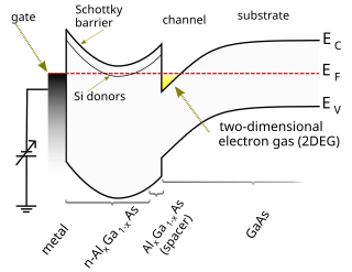
A high-electron-mobility transistor, also known as heterostructure FET (HFET) or modulation-doped FET (MODFET), is a field-effect transistor incorporating a junction between two materials with different band gaps as the channel instead of a doped region. A commonly used material combination is GaAs with AlGaAs, though there is wide variation, dependent on the application of the device. Devices incorporating more indium generally show better high-frequency performance, while in recent years, gallium nitride HEMTs have attracted attention due to their high-power performance.

Aluminium nitride (AlN) is a solid nitride of aluminium. It has a high thermal conductivity of up to 321 W/(m·K) and is an electrical insulator. Its wurtzite phase (w-AlN) has a band gap of ~6 eV at room temperature and has a potential application in optoelectronics operating at deep ultraviolet frequencies.

Trimethylaluminium is one of the simplest examples of an organoaluminium compound. Despite its name it has the formula Al2(CH3)6 (abbreviated as Al2Me6 or TMA), as it exists as a dimer. This colorless liquid is pyrophoric. It is an industrially important compound, closely related to triethylaluminium.
A heterojunction bipolar transistor (HBT) is a type of bipolar junction transistor (BJT) that uses different semiconductor materials for the emitter and base regions, creating a heterojunction. The HBT improves on the BJT in that it can handle signals of very high frequencies, up to several hundred GHz. It is commonly used in modern ultrafast circuits, mostly radio frequency (RF) systems, and in applications requiring a high power efficiency, such as RF power amplifiers in cellular phones. The idea of employing a heterojunction is as old as the conventional BJT, dating back to a patent from 1951. Detailed theory of heterojunction bipolar transistor was developed by Herbert Kroemer in 1957.

Indium nitride is a small bandgap semiconductor material which has potential application in solar cells and high speed electronics.

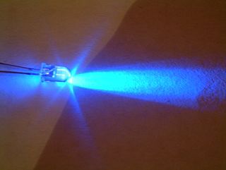
A blue laser emits electromagnetic radiation with a wavelength between 400 and 500 nanometers, which the human eye sees in the visible spectrum as blue or violet.
Indium gallium phosphide (InGaP), also called gallium indium phosphide (GaInP), is a semiconductor composed of indium, gallium and phosphorus. It is used in high-power and high-frequency electronics because of its superior electron velocity with respect to the more common semiconductors silicon and gallium arsenide.

Metalorganic vapour-phase epitaxy (MOVPE), also known as organometallic vapour-phase epitaxy (OMVPE) or metalorganic chemical vapour deposition (MOCVD), is a chemical vapour deposition method used to produce single- or polycrystalline thin films. It is a process for growing crystalline layers to create complex semiconductor multilayer structures. In contrast to molecular-beam epitaxy (MBE), the growth of crystals is by chemical reaction and not physical deposition. This takes place not in vacuum, but from the gas phase at moderate pressures. As such, this technique is preferred for the formation of devices incorporating thermodynamically metastable alloys, and it has become a major process in the manufacture of optoelectronics, such as light-emitting diodes, its most widespread application. It was first demonstrated in 1967 at North American Aviation Autonetics Division in Anaheim CA by Harold M. Manasevit.

Indium gallium nitride is a semiconductor material made of a mix of gallium nitride (GaN) and indium nitride (InN). It is a ternary group III/group V direct bandgap semiconductor. Its bandgap can be tuned by varying the amount of indium in the alloy. InxGa1−xN has a direct bandgap span from the infrared for InN to the ultraviolet of GaN. The ratio of In/Ga is usually between 0.02/0.98 and 0.3/0.7.
Aluminium gallium indium phosphide is a semiconductor material that provides a platform for the development of multi-junction photovoltaics and optoelectronic devices. It has a direct bandgap ranging from ultraviolet to infrared photon energies.
Aluminium gallium nitride (AlGaN) is a semiconductor material. It is any alloy of aluminium nitride and gallium nitride.
Aluminium indium arsenide, also indium aluminium arsenide or AlInAs (AlxIn1−xAs), is a ternary III-V semiconductor compound with very nearly the same lattice constant as InGaAs, but a larger bandgap. It can be considered as an alloy between aluminium arsenide (AlAs) and indium arsenide (InAs). AlInAs refers generally to any composition of the alloy.

Indium(III) oxide (In2O3) is a chemical compound, an amphoteric oxide of indium.
A quantum-well laser is a laser diode in which the active region of the device is so narrow that quantum confinement occurs. Laser diodes are formed in compound semiconductor materials that are able to emit light efficiently. The wavelength of the light emitted by a quantum-well laser is determined by the width of the active region rather than just the bandgap of the materials from which it is constructed. This means that much shorter wavelengths can be obtained from quantum-well lasers than from conventional laser diodes using a particular semiconductor material. The efficiency of a quantum-well laser is also greater than a conventional laser diode due to the stepwise form of its density of states function.
IQE PLC is a British semiconductor company founded 1988 in Cardiff, Wales, which manufactures advanced epitaxial wafers.

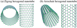
Gallium nitride nanotubes (GaNNTs) are nanotubes of gallium nitride. They can be grown by chemical vapour deposition.
Indium aluminium nitride (InAlN) is a direct bandgap semiconductor material used in the manufacture of electronic and photonic devices. It is part of the III-V group of semiconductors, being an alloy of indium nitride and aluminium nitride, and is closely related to the more widely used gallium nitride. It is of special interest in applications requiring good stability and reliability, owing to its large direct bandgap and ability to maintain operation at temperatures of up to 1000 °C., making it of particular interest to areas such as the space industry. InAlN high-electron-mobility transistors (HEMTs) are attractive candidates for such applications owing to the ability of InAlN to lattice-match to gallium nitride, eliminating a reported failure route in the closely related aluminium gallium nitride HEMTs.

