A semiconductor is a material that has an electrical conductivity value falling between that of a conductor, such as copper, and an insulator, such as glass. Its resistivity generally falls as its temperature rises; metals behave in the opposite way. In many cases their conducting properties may be altered in useful ways by introducing impurities ("doping") into the crystal structure. When two differently doped regions exist in the same crystal, a semiconductor junction is created. The behavior of charge carriers, which include electrons, ions, and electron holes, at these junctions is the basis of diodes, transistors, and most modern electronics. Some examples of semiconductors are silicon, germanium, gallium arsenide, and elements near the so-called "metalloid staircase" on the periodic table. After silicon, gallium arsenide is the second-most common semiconductor and is used in laser diodes, solar cells, microwave-frequency integrated circuits, and others. Silicon is a critical element for fabricating most electronic circuits.
Photoconductivity is an optical and electrical phenomenon in which a material becomes more electrically conductive due to the absorption of electromagnetic radiation such as visible light, ultraviolet light, infrared light, or gamma radiation.

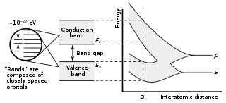
In solid-state physics and solid-state chemistry, a band gap, also called a bandgap or energy gap, is an energy range in a solid where no electronic states exist. In graphs of the electronic band structure of solids, the band gap refers to the energy difference between the top of the valence band and the bottom of the conduction band in insulators and semiconductors. It is the energy required to promote an electron from the valence band to the conduction band. The resulting conduction-band electron are free to move within the crystal lattice and serve as charge carriers to conduct electric current. It is closely related to the HOMO/LUMO gap in chemistry. If the valence band is completely full and the conduction band is completely empty, then electrons cannot move within the solid because there are no available states. If the electrons are not free to move within the crystal lattice, then there is no generated current due to no net charge carrier mobility. However, if some electrons transfer from the valence band to the conduction band, then current can flow. Therefore, the band gap is a major factor determining the electrical conductivity of a solid. Substances having large band gaps are generally insulators, those with small band gaps are semiconductor, and conductors either have very small band gaps or none, because the valence and conduction bands overlap to form a continuous band.

Gallium arsenide (GaAs) is a III-V direct band gap semiconductor with a zinc blende crystal structure.

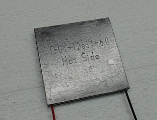
Thermoelectric materials show the thermoelectric effect in a strong or convenient form.
The photorefractive effect is a nonlinear optical effect seen in certain crystals and other materials that respond to light by altering their refractive index. The effect can be used to store temporary, erasable holograms and is useful for holographic data storage. It can also be used to create a phase-conjugate mirror or an optical spatial soliton.

Cadmium arsenide (Cd3As2) is an inorganic semimetal in the II-V family. It exhibits the Nernst effect.
In solid-state physics, the electron mobility characterises how quickly an electron can move through a metal or semiconductor when pushed or pulled by an electric field. There is an analogous quantity for holes, called hole mobility. The term carrier mobility refers in general to both electron and hole mobility.

In semiconductor production, doping is the intentional introduction of impurities into an intrinsic (undoped) semiconductor for the purpose of modulating its electrical, optical and structural properties. The doped material is referred to as an extrinsic semiconductor.
Organic semiconductors are solids whose building blocks are pi-bonded molecules or polymers made up by carbon and hydrogen atoms and – at times – heteroatoms such as nitrogen, sulfur and oxygen. They exist in the form of molecular crystals or amorphous thin films. In general, they are electrical insulators, but become semiconducting when charges are either injected from appropriate electrodes, upon doping or by photoexcitation.

Arsenic trisulfide is the inorganic compound with the formula As2S3. It is a dark yellow solid that is insoluble in water. It also occurs as the mineral orpiment, which has been used as a pigment called King's yellow. It is produced in the analysis of arsenic compounds. It is a group V/VI, intrinsic p-type semiconductor and exhibits photo-induced phase-change properties.
Chalcogenide glass is a glass containing one or more chalcogens. Polonium is also a chalcogen but is not used because of its strong radioactivity. Chalcogenide materials behave rather differently from oxides, in particular their lower band gaps contribute to very dissimilar optical and electrical properties.

In materials science, a single crystal is a material in which the crystal lattice of the entire sample is continuous and unbroken to the edges of the sample, with no grain boundaries. The absence of the defects associated with grain boundaries can give monocrystals unique properties, particularly mechanical, optical and electrical, which can also be anisotropic, depending on the type of crystallographic structure. These properties, in addition to making some gems precious, are industrially used in technological applications, especially in optics and electronics.
An extrinsic semiconductor is one that has been doped; during manufacture of the semiconductor crystal a trace element or chemical called a doping agent has been incorporated chemically into the crystal, for the purpose of giving it different electrical properties than the pure semiconductor crystal, which is called an intrinsic semiconductor. In an extrinsic semiconductor it is these foreign dopant atoms in the crystal lattice that mainly provide the charge carriers which carry electric current through the crystal. The doping agents used are of two types, resulting in two types of extrinsic semiconductor. An electron donor dopant is an atom which, when incorporated in the crystal, releases a mobile conduction electron into the crystal lattice. An extrinsic semiconductor that has been doped with electron donor atoms is called an n-type semiconductor, because the majority of charge carriers in the crystal are negative electrons. An electron acceptor dopant is an atom which accepts an electron from the lattice, creating a vacancy where an electron should be called a hole which can move through the crystal like a positively charged particle. An extrinsic semiconductor which has been doped with electron acceptor atoms is called a p-type semiconductor, because the majority of charge carriers in the crystal are positive holes.

Fluoride glass is a class of non-oxide optical glasses composed of fluorides of various metals. They can contain heavy metals such as zirconium, or be combined with lighter elements like aluminium and beryllium. These heavier elements cause the glass to have a transparency range extended into the infrared wavelength.

Transparent conducting films (TCFs) are thin films of optically transparent and electrically conductive material. They are an important component in a number of electronic devices including liquid-crystal displays, OLEDs, touchscreens and photovoltaics. While indium tin oxide (ITO) is the most widely used, alternatives include wider-spectrum transparent conductive oxides (TCOs), conductive polymers, metal grids and random metallic networks, carbon nanotubes (CNT), graphene, nanowire meshes and ultra thin metal films.
Organic photorefractive materials are materials that exhibit a temporary change in refractive index when exposed to light. The changing refractive index causes light to change speed throughout the material and produce light and dark regions in the crystal. The buildup can be controlled to produce holographic images for use in biomedical scans and optical computing. The ease with which the chemical composition can be changed in organic materials makes the photorefractive effect more controllable.
Two-photon photovoltaic effect is an energy collection method based on two-photon absorption (TPA). The TPP effect can be thought of as the nonlinear equivalent of the traditional photovoltaic effect involving high optical intensities. This effect occurs when two photons are absorbed at the same time resulting in an electron-hole pair.
Gallium lanthanum sulfide glass is the name of a family of chalcogenide glasses, referred to as gallium lanthanum sulfide (Ga-La-S) glasses. They are mixtures of La2S3, La2O3, and Ga2S3, which form the basic glass with other glass modifiers added as needed. Gallium-lanthanum-sulfide glasses have a wide range of vitreous formation centered around a 70% Ga2S3 : 30% La2S3 mixture, and readily accept other modifier materials into their structure. This means that Ga-La-S composition can be adjusted to give a wide variety of optical and physical properties.
Charge transport mechanisms are theoretical models that aim to quantitatively describe the electric current flow through a given medium.


