Niobium diselenide

Last updated
Niobium diselenide
2H NbSe2 structure.png
2H NbSe2 structure
NbSe2 STEM.jpg
Electron micrograph showing a local coexistence of different NbSe2 structures in one sample
Names
Other names
Niobium(IV) selenide
Identifiers
3D model (JSmol)
ChemSpider
ECHA InfoCard 100.031.634 OOjs UI icon edit-ltr-progressive.svg
EC Number
  • 234-811-8
PubChem CID
  • InChI=1S/Nb.2Se
    Key: CXRFFSKFQFGBOT-UHFFFAOYSA-N
  • [Se]=[Nb]=[Se]
Properties
NbSe2
Molar mass 250.83 g/mol [1]
AppearanceGray solid [1]
Density 6.3 g/cm3 [1]
Melting point >1300 °C [1]
Structure
hP6, space group P6
3
/mmc, No 194 [2]
a = 0.344 nm, c = 1.254 nm
Trigonal prismatic (NbIV)
Pyramidal (Se2−)
Related compounds
Other anions
Niobium dioxide
Other cations
Molybdenum diselenide
Tungsten diselenide
Except where otherwise noted, data are given for materials in their standard state (at 25 °C [77 °F], 100 kPa).

Niobium diselenide or niobium(IV) selenide is a layered transition metal dichalcogenide with formula NbSe2. Niobium diselenide is a lubricant, and a superconductor at temperatures below 7.2 K that exhibit a charge density wave (CDW). NbSe2 crystallizes in several related forms, and can be mechanically exfoliated into monatomic layers, similar to other transition metal dichalcogenide monolayers. Monolayer NbSe2 exhibits very different properties from the bulk material, such as of Ising superconductivity, quantum metallic state, and strong enhancement of the CDW. [3]

Contents

Synthesis

Number of NbSe2 layers as a function of Se powder temperature during CVD. NbSe2 thickness.png
Number of NbSe2 layers as a function of Se powder temperature during CVD.

Niobium diselenide crystals and thin films can be grown by chemical vapor deposition (CVD). Niobium oxide, selenium and NaCl powders are heated to different temperatures in the range 300–800 °C at ambient pressure in a furnace that allows maintaining a temperature gradient along its axis. Powders are placed in different locations in the furnace, and a mixture of argon and hydrogen is used as the carrier gas. The NbSe2 thickness can be accurately controlled by varying the temperature of selenium powder. [3]

NbSe2 monolayers can also be exfoliated from the bulk or deposited by molecular beam epitaxy. [3]

Structure

Niobium diselenide exists in several forms, including 1H, 2H, 4H and 3R, where H stands for hexagonal and R for rhombohedral, and the number 1, 2, etc., refers to the number of Se-Nb-Se layers in a unit cell. The Se-Nb-Se layers are bonded together with relatively weak van der Waals forces, and can be exfoliated into 1H monolayers. They can be offset in a variety of ways to make different crystal structures, the most stable being 2H. [4]

Properties

Superconductor

NbSe2 is a superconductor with a critical temperature TC = 7.2 K. [5] The critical temperature drops when the NbSe2 layers are intercalated by other atoms, or when the sample thickness decreases, with TC being ~1 K in a monolayer. [3] Recent studies show infrared photodetection in NbSe2 devices. [6]

Charge density wave

Along with the CDW the lattice develops a periodic lattice distortion around 26 K. This period is three times that of the crystal lattice, so that there is a 3 by 3 superlattice. [7] There is also a Cooper-pair density wave correlated but out of phase by 2π3 with the charge-density wave. [8]

Friction

NbSe2 sheets develop higher friction when very thin. [9]

Intercalation

Because the layers in NbSe2 are only weakly bonded together, different substances can penetrate between the layers to form well defined intercalation compounds. Compounds with helium, rubidium, transition metals, and post-transition metals have been made. Extra niobium atoms, up to one third extra can be added between the layers.

Extra metal atoms from first transition metal series can intercalate up to 1:3 ratio. they go in between the layers. [4]

Intercalating two atoms of helium per formula increases the layer separation to 2.9 and the Se-Se distance to 3.52. [10] [11]

Rubidium

When rubidium is intercalated, the NbSe2 layers separate to accommodate it. Each individual layer is also compressed slightly. The Nb-Se distance stays the same, but the Nb-Nb distance in the layer increases. The Se-Se distance on top and bottom of the layer decreases, and the Nb-Se-Nb angle increases. Extra electron density transfers from the Rb atoms to the niobium layer. [12]

Vanadium

Vanadium can enter the 2H NbSe2 structure to the limit of 1% by substituting for Nb. Between 11% and 20% it forms a 4Hb structure with V in octahedral coordination between layers. Over 30% it forms a 1T structure. [13]

Fermi energy is shifted into the d band. [14]

Iron

When doped with iron at levels greater than 8% NbSe2 can undergo a spin-glass transition at low temperatures. [15]

Hydrogen

Hydrogen can be intercalated into NbSe2 under high pressure and high temperature. Up to 0.9 atoms of hydrogen per formula can be included while retaining the same structure. Over this ratio the structure changes to that of MoS2. At this transition the crystallographic c-axis increases and paramagnetic susceptibility drops to zero. Hydrogen content can go to 5.2 molar ratio at 50.5 atmospheres. [16]

Magnesium

When magnesium is intercalated, the electron s-states do not overlap with the selenium, and it only has a small effect in reducing the superconducting critical temperature. [17]

Potential applications

Bemol Incorporated manufactured niobium diselenide in the United States for use as a conducting lubricant in vacuum, as it has a wide temperature stability range, very low outgassing, and lower resistance than graphite. NbSe2 was used as motor brushes, or embedded in silver to make a self lubricating surface. [18]

Related Research Articles

<span class="mw-page-title-main">High-temperature superconductivity</span> Superconductive behavior at temperatures much higher than absolute zero

High-temperature superconductors are defined as materials that behave as superconductors at temperatures above 77 K, the boiling point of liquid nitrogen. The adjective "high temperature" is only in respect to previously known superconductors, which function at even colder temperatures close to absolute zero. In absolute terms, these "high temperatures" are still far below ambient, and therefore require cooling. The first high-temperature superconductor was discovered in 1986, by IBM researchers Bednorz and Müller, who were awarded the Nobel Prize in Physics in 1987 "for their important break-through in the discovery of superconductivity in ceramic materials". Most high-Tc materials are type-II superconductors.

<span class="mw-page-title-main">Molybdenum disulfide</span> Chemical compound

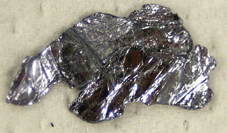
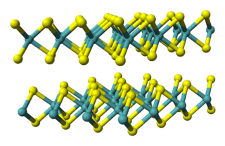
Molybdenum disulfide is an inorganic compound composed of molybdenum and sulfur. Its chemical formula is MoS
2
.

<span class="mw-page-title-main">Chalcogenide</span>

A chalcogenide is a chemical compound consisting of at least one chalcogen anion and at least one more electropositive element. Although all group 16 elements of the periodic table are defined as chalcogens, the term chalcogenide is more commonly reserved for sulfides, selenides, tellurides, and polonides, rather than oxides. Many metal ores exist as chalcogenides. Photoconductive chalcogenide glasses are used in xerography. Some pigments and catalysts are also based on chalcogenides. The metal dichalcogenide MoS2 is a common solid lubricant.

<span class="mw-page-title-main">Tungsten disulfide</span> Chemical compound

Tungsten disulfide is an inorganic chemical compound composed of tungsten and sulfur with the chemical formula WS2. This compound is part of the group of materials called the transition metal dichalcogenides. It occurs naturally as the rare mineral tungstenite. This material is a component of certain catalysts used for hydrodesulfurization and hydrodenitrification.

<span class="mw-page-title-main">Tungsten ditelluride</span> Chemical compound

Tungsten(IV) telluride (WTe2) is an inorganic semimetallic chemical compound. In October 2014, tungsten ditelluride was discovered to exhibit an extremely large magnetoresistance: 13 million percent resistance increase in a magnetic field of 60 Tesla at 0.5 Kelvin. The resistance is proportional to the square of the magnetic field and shows no saturation. This may be due to the material being the first example of a compensated semimetal, in which the number of mobile holes is the same as the number of electrons. Tungsten ditelluride has layered structure, similar to many other transition metal dichalcogenides, but its layers are so distorted that the honeycomb lattice many of them have in common is in WTe2 hard to recognize. The tungsten atoms instead form zigzag chains, which are thought to behave as one-dimensional conductors. Unlike electrons in other two dimensional semiconductors, the electrons in WTe2 can easily move between the layers.

<span class="mw-page-title-main">Tantalum(IV) sulfide</span> Chemical compound

Tantalum(IV) sulfide is an inorganic compound with the formula TaS2. It is a layered compound with three-coordinate sulfide centres and trigonal prismatic or octahedral metal centres. It is structurally similar to molybdenum disulfide MoS2, and numerous other transition metal dichalcogenide materials. The 1T-TaS2 polytype exhibits some unusual properties. In common with many other transition metal dichalcogenide (TMD) compounds, which are metallic at high temperatures, it exhibits a series of charge-density-wave (CDW) phase transitions from 550 K to 50 K. It is unusual amongst them in showing a low-temperature insulating state below 200 K, which is believed to arise from electron correlations, similar to many oxides. The insulating state is commonly attributed to a Mott state. It is also superconducting under pressure or upon doping, with a familiar dome-like phase diagram as a function of dopant, or substituted isovalent element concentration.

A charge density wave (CDW) is an ordered quantum fluid of electrons in a linear chain compound or layered crystal. The electrons within a CDW form a standing wave pattern and sometimes collectively carry an electric current. The electrons in such a CDW, like those in a superconductor, can flow through a linear chain compound en masse, in a highly correlated fashion. Unlike a superconductor, however, the electric CDW current often flows in a jerky fashion, much like water dripping from a faucet due to its electrostatic properties. In a CDW, the combined effects of pinning and electrostatic interactions likely play critical roles in the CDW current's jerky behavior, as discussed in sections 4 & 5 below.

<span class="mw-page-title-main">Niobium monoxide</span> Chemical compound

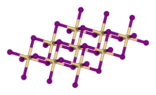
Niobium monoxide is the inorganic compound with the formula NbO. It is a grey solid with metallic conductivity.

<span class="mw-page-title-main">Titanium diselenide</span> Chemical compound

Titanium diselenide (TiSe2) also known as titanium(IV) selenide, is an inorganic compound of titanium and selenium. In this material selenium is viewed as selenide (Se2−) which requires that titanium exists as Ti4+. Titanium diselenide is a member of metal dichalcogenides, compounds that consist of a metal and an element of the chalcogen column within the periodic table. Many exhibit properties of potential value in battery technology, such as intercalation and electrical conductivity, although most applications focus on the less toxic and lighter disulfides, e.g. TiS2.

<span class="mw-page-title-main">Niobium triselenide</span> Chemical compound

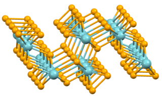
Niobium triselenide is an inorganic compound belonging to the class of transition metal trichalcogenides. It has the formula NbSe3. It was the first reported example of one-dimensional compound to exhibit the phenomenon of sliding charge density waves. Due to its many studies and exhibited phenomena in quantum mechanics, niobium triselenide has become the model system for quasi-1-D charge density waves.

<span class="mw-page-title-main">Molybdenum diselenide</span> Chemical compound

Molybdenum diselenide is an inorganic compound of molybdenum and selenium. Its structure is similar to that of MoS
2
. Compounds of this category are known as transition metal dichalcogenides, abbreviated TMDCs. These compounds, as the name suggests, are made up of a transition metals and elements of group 16 on the periodic table of the elements. Compared to MoS
2
, MoSe
2
exhibits higher electrical conductivity.

<span class="mw-page-title-main">Tungsten diselenide</span> Chemical compound

Tungsten diselenide is an inorganic compound with the formula WSe2. The compound adopts a hexagonal crystalline structure similar to molybdenum disulfide. Every tungsten atom is covalently bonded to six selenium ligands in a trigonal prismatic coordination sphere while each selenium is bonded to three tungsten atoms in a pyramidal geometry. The tungsten–selenium bond has a length of 0.2526 nm, and the distance between selenium atoms is 0.334 nm. It is a well studied example of a layered material. The layers stack together via van der Waals interactions. WSe2 is a very stable semiconductor in the group-VI transition metal dichalcogenides.

<span class="mw-page-title-main">Transition metal dichalcogenide monolayers</span> Thin semiconductors

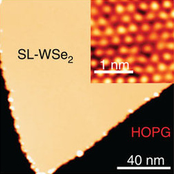
Transition-metal dichalcogenide (TMD or TMDC) monolayers are atomically thin semiconductors of the type MX2, with M a transition-metal atom (Mo, W, etc.) and X a chalcogen atom (S, Se, or Te). One layer of M atoms is sandwiched between two layers of X atoms. They are part of the large family of so-called 2D materials, named so to emphasize their extraordinary thinness. For example, a MoS2 monolayer is only 6.5 Å thick. The key feature of these materials is the interaction of large atoms in the 2D structure as compared with first-row transition-metal dichalcogenides, e.g., WTe2 exhibits anomalous giant magnetoresistance and superconductivity.

In materials science, the term single-layer materials or 2D materials refers to crystalline solids consisting of a single layer of atoms. These materials are promising for some applications but remain the focus of research. Single-layer materials derived from single elements generally carry the -ene suffix in their names, e.g. graphene. Single-layer materials that are compounds of two or more elements have -ane or -ide suffixes. 2D materials can generally be categorized as either 2D allotropes of various elements or as compounds.

<span class="mw-page-title-main">Molybdenum ditelluride</span> Chemical compound

Molybdenum(IV) telluride, molybdenum ditelluride or just molybdenum telluride is a compound of molybdenum and tellurium with formula MoTe2, corresponding to a mass percentage of 27.32% molybdenum and 72.68% tellurium. It can crystallise in two dimensional sheets which can be thinned down to monolayers that are flexible and almost transparent. It is a semiconductor, and can fluoresce. It is part of a class of materials called transition metal dichalcogenides. As a semiconductor the band gap lies in the infrared region. This raises the potential use as a semiconductor in electronics or an infrared detector.

Platinum diselenide is a transition metal dichalcogenide with the formula PtSe2. It is a layered substance that can be split into layers down to three atoms thick. PtSe2 can behave as a metalloid or as a semiconductor depending on the thickness.

Verbeekite is a rare mineral consisting of palladium diselenide PdSe2. This transition metal dichalcogenide has an unusual monoclinic structure, with pairs of selenium atoms existing as dimers forming layers between palladium atom sheets. Unit cell dimensions are: a = 6.710, b = 4.154, c = 8.914 Å, β = 92.42 °, V = 248.24 Å3. Palladium diselenide has five polymorphs. Verbeekite can be synthesised at 11.5 GPa pressure and 1300 °C.

<span class="mw-page-title-main">Rhenium diselenide</span> Chemical compound

Rhenium diselenide is an inorganic compound with the formula ReSe2. It has a layered structure where atoms are strongly bonded within each layer. The layers are held together by weak Van der Waals bonds, and can be easily peeled off from the bulk material.

<span class="mw-page-title-main">Niobium disulfide</span> Chemical compound

Niobium disulfide is the chemical compound with the formula NbS2. It is a black layered solid that can be exfoliated into ultrathin grayish sheets similar to other transition metal dichalcogenides. These layers exhibit superconductivity, where the transition temperature increases from ca. 2 to 6 K with the layer thickness increasing from 6 to 12 nm, and then saturates with thickness.

<span class="mw-page-title-main">Tantalum diselenide</span> Chemical compound

Tantalum diselenide is a compound made with tantalum and selenium atoms, with chemical formula TaSe2, which belongs to the family of transition metal dichalcogenides. In contrast to molybdenum disulfide (MoS2) or rhenium disulfide (ReS2, tantalum diselenide does not occur spontaneously in nature, but it can be synthesized. Depending on the growth parameters, different types of crystal structures can be stabilized.

References

  1. 1 2 3 4 Haynes, William M., ed. (2011). CRC Handbook of Chemistry and Physics (92nd ed.). Boca Raton, FL: CRC Press. p. 4.78. ISBN   1-4398-5511-0.
  2. Rajora, O. S; Curzon, A. E (1987). "The preparation and X-ray diffraction study of the layer materials NbSxSe2−x for 0 ≦ x ≦ 2". Physica Status Solidi A. 99 (1): 65. Bibcode:1987PSSAR..99...65R. doi:10.1002/pssa.2210990108.
  3. 1 2 3 4 Wang, Hong; Huang, Xiangwei; Lin, Junhao; Cui, Jian; Chen, Yu; Zhu, Chao; Liu, Fucai; Zeng, Qingsheng; Zhou, Jiadong; Yu, Peng; Wang, Xuewen; He, Haiyong; Tsang, Siu Hon; Gao, Weibo; Suenaga, Kazu; Ma, Fengcai; Yang, Changli; Lu, Li; Yu, Ting; Teo, Edwin Hang Tong; Liu, Guangtong; Liu, Zheng (2017). "High-quality monolayer superconductor NbSe2 grown by chemical vapour deposition". Nature Communications. 8 (1): 394. Bibcode:2017NatCo...8..394W. doi:10.1038/s41467-017-00427-5. PMC   5577275 . PMID   28855521.
  4. 1 2 Lévy, Francis (2012). Crystallography and Crystal Chemistry of Materials with Layered Structures. Springer Science & Business Media. pp. 9–12. ISBN   9789401014335.
  5. NbSe2, a true 2-D superconductor. Physorg (November 6, 2015)
  6. Orchin, G. J.; De Fazio, D.; Di Bernardo, A.; Hamer, M.; Yoon, D.; Cadore, A. R.; Goykhman, I.; Watanabe, K.; Taniguchi, T. (2019-06-24). "Niobium diselenide superconducting photodetectors". Applied Physics Letters. 114 (25): 251103. arXiv: 1903.02528 . Bibcode:2019ApPhL.114y1103O. doi:10.1063/1.5097389. ISSN   0003-6951. S2CID   119349265.
  7. Riccó, B. (1977). "Fermi surface and charge density waves in niobium diselenide". Solid State Communications. 22 (5): 331–333. Bibcode:1977SSCom..22..331R. doi:10.1016/0038-1098(77)91442-9.
  8. Liu, Xiaolong; Chong, Yi Xue; Sharma, Rahul; Davis, J. C. Séamus (2021-06-25). "Discovery of a Cooper-pair density wave state in a transition-metal dichalcogenide". Science. 372 (6549): 1447–1452. arXiv: 2007.15228 . doi:10.1126/science.abd4607. S2CID   220871205.
  9. "Nanoscale Frictional Characteristics Revealed" . Retrieved 25 March 2017.
  10. Birks, A. R.; Hind, S. P.; Lee, P. M. (1976). "Band Structure Changes in Interealates of Niobium Diselenide". Physica Status Solidi B. 76 (2): 599–604. Bibcode:1976PSSBR..76..599B. doi:10.1002/pssb.2220760219.
  11. Brown, Bruce E.; Beernsten, Donald J. (1965). "Layer structure polytypism among niobium and tantalum selenides" (PDF). Acta Crystallographica. 18: 31–38. doi: 10.1107/S0365110X65000063 .
  12. Bourdillon, A J; Pettifer, R F; Marseglia, E A (1979). "EXAFS in niobium diselenide intercalated with rubidium". Journal of Physics C: Solid State Physics. 12 (19): 3889–3897. Bibcode:1979JPhC...12.3889B. doi:10.1088/0022-3719/12/19/007.
  13. Bayard, Michel; Mentzen, Bernard F.; Sienko, M. J. (1976). "Synthesis and structural aspects of the vanadium-substituted niobium diselenides". Inorganic Chemistry. 15 (8): 1763–1767. doi:10.1021/ic50162a005.
  14. Ibrahem, Mohammed Aziz; Huang, Wei-Chih; Lan, Tian-wey; Boopathi, Karunakara Moorthy; Hsiao, Yu-Chen; Chen, Chih-Han; Budiawan, Widhya; Chen, Yang-Yuan; Chang, Chia-Seng; Li, Lain-Jong; Tsai, Chih-Hung; Chu, Chih Wei (2014). "Controlled mechanical cleavage of bulk niobium diselenide to nanoscaled sheet, rod, and particle structures for Pt-free dye-sensitized solar cells". Journal of Materials Chemistry A. 2 (29): 11382. doi:10.1039/c4ta01881h.
  15. Chen, M. C.; Slichter, C. P. (1 January 1983). "Zero-field NMR study on a spin-glass: Iron-doped—niobium diselenide". Physical Review B. 27 (1): 278–292. Bibcode:1983PhRvB..27..278C. doi:10.1103/PhysRevB.27.278. OSTI   5197013.
  16. Kulikov, Leonid M.; Lazorenko, Vasilii I.; Lashkarev, Georgii V. (2002). "Magnetic Susceptibility of Powders of Hydrogen Intercalates of Niobium Diselenide". Powder Metallurgy and Metal Ceramics. 41 (1/2): 107–111. doi:10.1023/A:1016076918474. S2CID   91726908.
  17. Naik, Subham; Kalaiarasan, Somesh; Nath, Ramesh C.; Sarangi, Sachindra N.; Sahu, Akshay K.; Samal, Debakanta; Biswal, Himansu S.; Samal, Saroj L. (10 March 2021). "Nominal Effect of Mg Intercalation on the Superconducting Properties of 2H–NbSe 2". Inorganic Chemistry. 60 (7): 4588–4598. doi:10.1021/acs.inorgchem.0c03545. PMID   33689330. S2CID   232197802.
  18. Anglo Bell Company (October 1965). "Niobium diselenide lubricant". Vacuum. 15 (10): 511. doi:10.1016/0042-207X(65)90361-1.