A request that this article title be changed to AMD APU is under discussion. Please do not move this article until the discussion is closed. |
This article may contain an excessive amount of intricate detail that may interest only a particular audience.(April 2021) |
Release date | 2011 (Original); 2017 (Zen based) |
---|---|
Codename | Fusion Desna Ontario Zacate Llano Hondo Trinity Weatherford Richland Kaveri Godavari Kabini Temash Carrizo Bristol Ridge Raven Ridge Picasso Renoir Cezanne IGP Wrestler WinterPark BeaverCreek |
Architecture | AMD64 |
Models |
|
Cores | 1 to 8 |
Transistors |
|
API support | |
Direct3D | Direct3D 11 Direct3D 12 |
OpenCL | 1.2 |
OpenGL | 4.1+ |
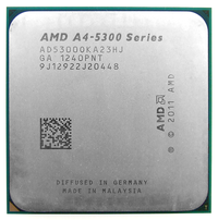
AMD Accelerated Processing Unit (APU), formerly known as Fusion, is a series of 64-bit microprocessors from Advanced Micro Devices (AMD), combining a general-purpose AMD64 central processing unit (CPU) and 3D integrated graphics processing unit (IGPU) on a single die.
AMD announced the first generation APUs, Llano for high-performance and Brazos for low-power devices, in January 2011. The second generation Trinity for high-performance and Brazos-2 for low-power devices were announced in June 2012. The third generation Kaveri for high performance devices were launched in January 2014, while Kabini and Temash for low-power devices were announced in the summer of 2013. Since the launch of the Zen microarchitecture, Ryzen and Athlon APUs have released to the global market as Raven Ridge on the DDR4 platform, after Bristol Ridge a year prior.
AMD has also supplied semi-custom APUs for consoles starting with the release of Sony PlayStation 4 and Microsoft Xbox One eighth generation video game consoles.
The AMD Fusion project started in 2006 with the aim of developing a system on a chip that combined a CPU with a GPU on a single die. This effort was moved forward by AMD's acquisition of graphics chipset manufacturer ATI [1] in 2006. The project reportedly required three internal iterations of the Fusion concept to create a product deemed worthy of release. [1] Reasons contributing to the delay of the project include the technical difficulties of combining a CPU and GPU on the same die at a 45 nm process, and conflicting views on what the role of the CPU and GPU should be within the project. [2]
The first generation desktop and laptop APU, codenamed Llano, was announced on 4 January 2011 at the 2011 CES show in Las Vegas and released shortly thereafter. [3] [4] It featured K10 CPU cores and a Radeon HD 6000 series GPU on the same die on the FM1 socket. An APU for low-power devices was announced as the Brazos platform, based on the Bobcat microarchitecture and a Radeon HD 6000 series GPU on the same die. [5]
At a conference in January 2012, corporate fellow Phil Rogers announced that AMD would re-brand the Fusion platform as the Heterogeneous System Architecture (HSA), stating that "it's only fitting that the name of this evolving architecture and platform be representative of the entire, technical community that is leading the way in this very important area of technology and programming development." [6] However, it was later revealed that AMD had been the subject of a trademark infringement lawsuit by the Swiss company Arctic, who used the name "Fusion" for a line of power supply products. [7]
The second generation desktop and laptop APU, codenamed Trinity was announced at AMD's 2010 Financial Analyst Day [8] [9] and released in October 2012. [10] It featured Piledriver CPU cores and Radeon HD 7000 series GPU cores on the FM2 socket. [11] AMD released a new APU based on the Piledriver microarchitecture on 12 March 2013 for Laptops/Mobile and on 4 June 2013 for desktops under the codename Richland. [12] The second generation APU for low-power devices, Brazos 2.0, used exactly the same APU chip, but ran at higher clock speed and rebranded the GPU as Radeon HD 7000 series and used a new I/O controller chip.
Semi-custom chips were introduced in the Microsoft Xbox One and Sony PlayStation 4 video game consoles, [13] [14] and subsequently in the Microsoft Xbox Series X|S and Sony PlayStation 5 consoles.
A third generation of the technology was released on 14 January 2014, featuring greater integration between CPU and GPU. The desktop and laptop variant is codenamed Kaveri, based on the Steamroller architecture, while the low-power variants, codenamed Kabini and Temash, are based on the Jaguar architecture. [15]
Since the introduction of Zen-based processors, AMD renamed their APUs as the Ryzen with Radeon Graphics and Athlon with Radeon Graphics, with desktop units assigned with G suffix on their model numbers (e.g. Ryzen 5 3400G & Athlon 3000G) to distinguish them from regular processors or with basic graphics and also to differentiate away from their former Bulldozer era A-series APUs. The mobile counterparts were always paired with Radeon Graphics regardless of suffixes.
In November 2017, HP released the Envy x360, featuring the Ryzen 5 2500U APU, the first 4th generation APU, based on the Zen CPU architecture and the Vega graphics architecture. [16]
AMD is a founding member of the Heterogeneous System Architecture (HSA) Foundation and is consequently actively working on developing HSA in cooperation with other members. The following hardware and software implementations are available in AMD's APU-branded products:
Type | HSA feature | First implemented | Notes |
---|---|---|---|
Optimized Platform | GPU Compute C++ Support | 2012 Trinity APUs | Support OpenCL C++ directions and Microsoft's C++ AMP language extension. This eases programming of both CPU and GPU working together to process support parallel workloads. |
HSA-aware MMU | GPU can access the entire system memory through the translation services and page fault management of the HSA MMU. | ||
Shared Power Management | CPU and GPU now share the power budget. Priority goes to the processor most suited to the current tasks. | ||
Architectural Integration | Heterogeneous Memory Management: the CPU's MMU and the GPU's IOMMU share the same address space. [17] [18] | 2014 PlayStation 4, Kaveri APUs | CPU and GPU now access the memory with the same address space. Pointers can now be freely passed between CPU and GPU, hence enabling zero-copy . |
Fully coherent memory between CPU and GPU | GPU can now access and cache data from coherent memory regions in the system memory, and also reference the data from CPU's cache. Cache coherency is maintained. | ||
GPU uses pageable system memory via CPU pointers | GPU can take advantage of the shared virtual memory between CPU and GPU, and pageable system memory can now be referenced directly by the GPU, instead of being copied or pinned before accessing. | ||
System Integration | GPU compute context switch | 2015 Carrizo APU | Compute tasks on GPU can be context switched, allowing a multi-tasking environment and also faster interpretation between applications, compute and graphics. |
GPU graphics pre-emption | Long-running graphics tasks can be pre-empted so processes have low latency access to the GPU. | ||
Quality of service [17] | In addition to context switch and pre-emption, hardware resources can be either equalized or prioritized among multiple users and applications. |
The following table shows features of AMD's processors with 3D graphics, including APUs (see also: List of AMD Processors with 3D Graphics).
Platform | High, standard and low power | Low and ultra-low power | ||||||||||||||||||||||||||||||||||||||||||||||||||||||||||||||||||||||||||||||||||||||||||||||||||
---|---|---|---|---|---|---|---|---|---|---|---|---|---|---|---|---|---|---|---|---|---|---|---|---|---|---|---|---|---|---|---|---|---|---|---|---|---|---|---|---|---|---|---|---|---|---|---|---|---|---|---|---|---|---|---|---|---|---|---|---|---|---|---|---|---|---|---|---|---|---|---|---|---|---|---|---|---|---|---|---|---|---|---|---|---|---|---|---|---|---|---|---|---|---|---|---|---|---|---|---|
Codename | Server | Basic | Toronto | |||||||||||||||||||||||||||||||||||||||||||||||||||||||||||||||||||||||||||||||||||||||||||||||||
Micro | Kyoto | |||||||||||||||||||||||||||||||||||||||||||||||||||||||||||||||||||||||||||||||||||||||||||||||||||
Desktop | Performance | Raphael | ||||||||||||||||||||||||||||||||||||||||||||||||||||||||||||||||||||||||||||||||||||||||||||||||||
Mainstream | Llano | Trinity | Richland | Kaveri | Kaveri Refresh (Godavari) | Carrizo | Bristol Ridge | Raven Ridge | Picasso | Renoir | Cezanne | |||||||||||||||||||||||||||||||||||||||||||||||||||||||||||||||||||||||||||||||||||||||||
Entry | ||||||||||||||||||||||||||||||||||||||||||||||||||||||||||||||||||||||||||||||||||||||||||||||||||||
Basic | Kabini | Dalí | ||||||||||||||||||||||||||||||||||||||||||||||||||||||||||||||||||||||||||||||||||||||||||||||||||
Mobile | Performance | Renoir | Cezanne | Rembrandt | Dragon Range | |||||||||||||||||||||||||||||||||||||||||||||||||||||||||||||||||||||||||||||||||||||||||||||||
Mainstream | Llano | Trinity | Richland | Kaveri | Carrizo | Bristol Ridge | Raven Ridge | Picasso | Renoir Lucienne | Cezanne Barceló | ||||||||||||||||||||||||||||||||||||||||||||||||||||||||||||||||||||||||||||||||||||||||||
Entry | Dalí | Mendocino | ||||||||||||||||||||||||||||||||||||||||||||||||||||||||||||||||||||||||||||||||||||||||||||||||||
Basic | Desna, Ontario, Zacate | Kabini, Temash | Beema, Mullins | Carrizo-L | Stoney Ridge | Pollock | ||||||||||||||||||||||||||||||||||||||||||||||||||||||||||||||||||||||||||||||||||||||||||||||
Embedded | Trinity | Bald Eagle | Merlin Falcon, Brown Falcon | Great Horned Owl | Grey Hawk | Ontario, Zacate | Kabini | Steppe Eagle, Crowned Eagle, LX-Family | Prairie Falcon | Banded Kestrel | River Hawk | |||||||||||||||||||||||||||||||||||||||||||||||||||||||||||||||||||||||||||||||||||||||||
Released | Aug 2011 | Oct 2012 | Jun 2013 | Jan 2014 | 2015 | Jun 2015 | Jun 2016 | Oct 2017 | Jan 2019 | Mar 2020 | Jan 2021 | Jan 2022 | Sep 2022 | Jan 2011 | May 2013 | Apr 2014 | May 2015 | Feb 2016 | Apr 2019 | Jul 2020 | Jun 2022 | Nov 2022 | ||||||||||||||||||||||||||||||||||||||||||||||||||||||||||||||||||||||||||||||
CPU microarchitecture | K10 | Piledriver | Steamroller | Excavator | "Excavator+" [19] | Zen | Zen+ | Zen 2 | Zen 3 | Zen 3+ | Zen 4 | Bobcat | Jaguar | Puma | Puma+ [20] | "Excavator+" | Zen | Zen+ | "Zen 2+" | |||||||||||||||||||||||||||||||||||||||||||||||||||||||||||||||||||||||||||||||||
ISA | x86-64 v1 | x86-64 v2 | x86-64 v3 | x86-64 v4 | x86-64 v1 | x86-64 v2 | x86-64 v3 | |||||||||||||||||||||||||||||||||||||||||||||||||||||||||||||||||||||||||||||||||||||||||||||
Socket | Desktop | Performance | — | AM5 | — | |||||||||||||||||||||||||||||||||||||||||||||||||||||||||||||||||||||||||||||||||||||||||||||||
Mainstream | — | AM4 | — | |||||||||||||||||||||||||||||||||||||||||||||||||||||||||||||||||||||||||||||||||||||||||||||||||
Entry | FM1 | FM2 | FM2+ | FM2+ [lower-alpha 1] , AM4 | AM4 | — | ||||||||||||||||||||||||||||||||||||||||||||||||||||||||||||||||||||||||||||||||||||||||||||||
Basic | — | — | AM1 | — | FP5 | — | ||||||||||||||||||||||||||||||||||||||||||||||||||||||||||||||||||||||||||||||||||||||||||||||
Other | FS1 | FS1+, FP2 | FP3 | FP4 | FP5 | FP6 | FP7 | ? | FT1 | FT3 | FT3b | FP4 | FP5 | FT5 | FP5 | FT6 | ||||||||||||||||||||||||||||||||||||||||||||||||||||||||||||||||||||||||||||||||||||
PCI Express version | 2.0 | 3.0 | 4.0 | 5.0 | 2.0 | 3.0 | ||||||||||||||||||||||||||||||||||||||||||||||||||||||||||||||||||||||||||||||||||||||||||||||
CXL | — | — | ||||||||||||||||||||||||||||||||||||||||||||||||||||||||||||||||||||||||||||||||||||||||||||||||||
Fab. (nm) | GF 32SHP (HKMG SOI) | GF 28SHP (HKMG bulk) | GF 14LPP (FinFET bulk) | GF 12LP (FinFET bulk) | TSMC N7 (FinFET bulk) | TSMC N6 (FinFET bulk) | CCD: TSMC N5 (FinFET bulk) cIOD: TSMC N6 (FinFET bulk) | TSMC N40 (bulk) | TSMC N28 (HKMG bulk) | GF 28SHP (HKMG bulk) | GF 14LPP (FinFET bulk) | GF 12LP (FinFET bulk) | TSMC N6 (FinFET bulk) | |||||||||||||||||||||||||||||||||||||||||||||||||||||||||||||||||||||||||||||||||||||||
Die area (mm2) | 228 | 246 | 245 | 245 | 250 | 210 [21] | 156 | 180 | 210 | 75 (+ 28 FCH) | 107 | ? | 125 | 149 | ||||||||||||||||||||||||||||||||||||||||||||||||||||||||||||||||||||||||||||||||||||||
Min TDP (W) | 35 | 17 | 12 | 10 | 15 | 105 | 4.5 | 4 | 3.95 | 10 | 6 | 12 | 8 | |||||||||||||||||||||||||||||||||||||||||||||||||||||||||||||||||||||||||||||||||||||||
Max APU TDP (W) | 100 | 95 | 65 | 45 | 170 | 18 | 25 | 6 | 54 | 15 | ||||||||||||||||||||||||||||||||||||||||||||||||||||||||||||||||||||||||||||||||||||||||||
Max stock APU base clock (GHz) | 3 | 3.8 | 4.1 | 4.1 | 3.7 | 3.8 | 3.6 | 3.7 | 3.8 | 4.0 | 3.3 | 4.7 | 1.75 | 2.2 | 2 | 2.2 | 3.2 | 2.6 | 1.2 | 3.35 | 2.8 | |||||||||||||||||||||||||||||||||||||||||||||||||||||||||||||||||||||||||||||||
Max APUs per node [lower-alpha 2] | 1 | 1 | ||||||||||||||||||||||||||||||||||||||||||||||||||||||||||||||||||||||||||||||||||||||||||||||||||
Max core dies per CPU | 1 | 2 | 1 | |||||||||||||||||||||||||||||||||||||||||||||||||||||||||||||||||||||||||||||||||||||||||||||||||
Max CCX per core die | 1 | 2 | 1 | 1 | ||||||||||||||||||||||||||||||||||||||||||||||||||||||||||||||||||||||||||||||||||||||||||||||||
Max cores per CCX | 4 | 8 | 2 | 4 | 2 | 4 | ||||||||||||||||||||||||||||||||||||||||||||||||||||||||||||||||||||||||||||||||||||||||||||||
Max CPU [lower-alpha 3] cores per APU | 4 | 8 | 16 | 2 | 4 | 2 | 4 | |||||||||||||||||||||||||||||||||||||||||||||||||||||||||||||||||||||||||||||||||||||||||||||
Max threads per CPU core | 1 | 2 | 1 | 2 | ||||||||||||||||||||||||||||||||||||||||||||||||||||||||||||||||||||||||||||||||||||||||||||||||
Integer pipeline structure | 3+3 | 2+2 | 4+2 | 4+2+1 | 1+3+3+1+2 | 1+1+1+1 | 2+2 | 4+2 | 4+2+1 | |||||||||||||||||||||||||||||||||||||||||||||||||||||||||||||||||||||||||||||||||||||||||||
i386, i486, i586, CMOV, NOPL, i686, PAE, NX bit, CMPXCHG16B, AMD-V, RVI, ABM, and 64-bit LAHF/SAHF | ||||||||||||||||||||||||||||||||||||||||||||||||||||||||||||||||||||||||||||||||||||||||||||||||||||
IOMMU [lower-alpha 4] | — | v2 | v1 | v2 | ||||||||||||||||||||||||||||||||||||||||||||||||||||||||||||||||||||||||||||||||||||||||||||||||
BMI1, AES-NI, CLMUL, and F16C | — | |||||||||||||||||||||||||||||||||||||||||||||||||||||||||||||||||||||||||||||||||||||||||||||||||||
MOVBE | — | |||||||||||||||||||||||||||||||||||||||||||||||||||||||||||||||||||||||||||||||||||||||||||||||||||
AVIC, BMI2, RDRAND, and MWAITX/MONITORX | — | |||||||||||||||||||||||||||||||||||||||||||||||||||||||||||||||||||||||||||||||||||||||||||||||||||
SME [lower-alpha 5] , TSME [lower-alpha 5] , ADX, SHA, RDSEED, SMAP, SMEP, XSAVEC, XSAVES, XRSTORS, CLFLUSHOPT, CLZERO, and PTE Coalescing | — | — | ||||||||||||||||||||||||||||||||||||||||||||||||||||||||||||||||||||||||||||||||||||||||||||||||||
GMET, WBNOINVD, CLWB, QOS, PQE-BW, RDPID, RDPRU, and MCOMMIT | — | — | ||||||||||||||||||||||||||||||||||||||||||||||||||||||||||||||||||||||||||||||||||||||||||||||||||
MPK, VAES | — | — | ||||||||||||||||||||||||||||||||||||||||||||||||||||||||||||||||||||||||||||||||||||||||||||||||||
SGX | — | — | ||||||||||||||||||||||||||||||||||||||||||||||||||||||||||||||||||||||||||||||||||||||||||||||||||
FPUs per core | 1 | 0.5 | 1 | 1 | 0.5 | 1 | ||||||||||||||||||||||||||||||||||||||||||||||||||||||||||||||||||||||||||||||||||||||||||||||
Pipes per FPU | 2 | 2 | ||||||||||||||||||||||||||||||||||||||||||||||||||||||||||||||||||||||||||||||||||||||||||||||||||
FPU pipe width | 128-bit | 256-bit | 80-bit | 128-bit | 256-bit | |||||||||||||||||||||||||||||||||||||||||||||||||||||||||||||||||||||||||||||||||||||||||||||||
CPU instruction set SIMD level | SSE4a [lower-alpha 6] | AVX | AVX2 | AVX-512 | SSSE3 | AVX | AVX2 | |||||||||||||||||||||||||||||||||||||||||||||||||||||||||||||||||||||||||||||||||||||||||||||
3DNow! | 3DNow!+ | — | — | |||||||||||||||||||||||||||||||||||||||||||||||||||||||||||||||||||||||||||||||||||||||||||||||||
PREFETCH/PREFETCHW | ||||||||||||||||||||||||||||||||||||||||||||||||||||||||||||||||||||||||||||||||||||||||||||||||||||
GFNI | — | — | ||||||||||||||||||||||||||||||||||||||||||||||||||||||||||||||||||||||||||||||||||||||||||||||||||
AMX | — | |||||||||||||||||||||||||||||||||||||||||||||||||||||||||||||||||||||||||||||||||||||||||||||||||||
FMA4, LWP, TBM, and XOP | — | — | — | — | ||||||||||||||||||||||||||||||||||||||||||||||||||||||||||||||||||||||||||||||||||||||||||||||||
FMA3 | ||||||||||||||||||||||||||||||||||||||||||||||||||||||||||||||||||||||||||||||||||||||||||||||||||||
L1 data cache per core (KiB) | 64 | 16 | 32 | 32 | ||||||||||||||||||||||||||||||||||||||||||||||||||||||||||||||||||||||||||||||||||||||||||||||||
L1 data cache associativity (ways) | 2 | 4 | 8 | 8 | ||||||||||||||||||||||||||||||||||||||||||||||||||||||||||||||||||||||||||||||||||||||||||||||||
L1 instruction caches per core | 1 | 0.5 | 1 | 1 | 0.5 | 1 | ||||||||||||||||||||||||||||||||||||||||||||||||||||||||||||||||||||||||||||||||||||||||||||||
Max APU total L1 instruction cache (KiB) | 256 | 128 | 192 | 256 | 512 | 64 | 128 | 96 | 128 | |||||||||||||||||||||||||||||||||||||||||||||||||||||||||||||||||||||||||||||||||||||||||||
L1 instruction cache associativity (ways) | 2 | 3 | 4 | 8 | 2 | 3 | 4 | 8 | ||||||||||||||||||||||||||||||||||||||||||||||||||||||||||||||||||||||||||||||||||||||||||||
L2 caches per core | 1 | 0.5 | 1 | 1 | 0.5 | 1 | ||||||||||||||||||||||||||||||||||||||||||||||||||||||||||||||||||||||||||||||||||||||||||||||
Max APU total L2 cache (MiB) | 4 | 2 | 4 | 16 | 1 | 2 | 1 | 2 | ||||||||||||||||||||||||||||||||||||||||||||||||||||||||||||||||||||||||||||||||||||||||||||
L2 cache associativity (ways) | 16 | 8 | 16 | 8 | ||||||||||||||||||||||||||||||||||||||||||||||||||||||||||||||||||||||||||||||||||||||||||||||||
Max on--die L3 cache per CCX (MiB) | — | 4 | 16 | 32 | — | 4 | ||||||||||||||||||||||||||||||||||||||||||||||||||||||||||||||||||||||||||||||||||||||||||||||
Max 3D V-Cache per CCD (MiB) | — | 64 | — | |||||||||||||||||||||||||||||||||||||||||||||||||||||||||||||||||||||||||||||||||||||||||||||||||
Max total in-CCD L3 cache per APU (MiB) | 4 | 8 | 16 | 64 | 4 | |||||||||||||||||||||||||||||||||||||||||||||||||||||||||||||||||||||||||||||||||||||||||||||||
Max. total 3D V-Cache per APU (MiB) | — | 64 | — | |||||||||||||||||||||||||||||||||||||||||||||||||||||||||||||||||||||||||||||||||||||||||||||||||
Max. board L3 cache per APU (MiB) | — | — | ||||||||||||||||||||||||||||||||||||||||||||||||||||||||||||||||||||||||||||||||||||||||||||||||||
Max total L3 cache per APU (MiB) | 4 | 8 | 16 | 128 | 4 | |||||||||||||||||||||||||||||||||||||||||||||||||||||||||||||||||||||||||||||||||||||||||||||||
APU L3 cache associativity (ways) | 16 | 16 | ||||||||||||||||||||||||||||||||||||||||||||||||||||||||||||||||||||||||||||||||||||||||||||||||||
L3 cache scheme | Victim | Victim | ||||||||||||||||||||||||||||||||||||||||||||||||||||||||||||||||||||||||||||||||||||||||||||||||||
Max. L4 cache | — | — | ||||||||||||||||||||||||||||||||||||||||||||||||||||||||||||||||||||||||||||||||||||||||||||||||||
Max stock DRAM support | DDR3-1866 | DDR3-2133 | DDR3-2133, DDR4-2400 | DDR4-2400 | DDR4-2933 | DDR4-3200, LPDDR4-4266 | DDR5-4800, LPDDR5-6400 | DDR5-5200 | DDR3L-1333 | DDR3L-1600 | DDR3L-1866 | DDR3-1866, DDR4-2400 | DDR4-2400 | DDR4-1600 | DDR4-3200 | LPDDR5-5500 | ||||||||||||||||||||||||||||||||||||||||||||||||||||||||||||||||||||||||||||||||||||
Max DRAM channels per APU | 2 | 1 | 2 | 1 | 2 | |||||||||||||||||||||||||||||||||||||||||||||||||||||||||||||||||||||||||||||||||||||||||||||||
Max stock DRAM bandwidth (GB/s) per APU | 29.866 | 34.132 | 38.400 | 46.932 | 68.256 | 102.400 | 83200 | 10.666 | 12.800 | 14.933 | 19.200 | 38.400 | 12.800 | 51.200 | 88.000 | |||||||||||||||||||||||||||||||||||||||||||||||||||||||||||||||||||||||||||||||||||||
GPU microarchitecture | TeraScale 2 (VLIW5) | TeraScale 3 (VLIW4) | GCN 2nd gen | GCN 3rd gen | GCN 5th gen [22] | RDNA 2nd gen | TeraScale 2 (VLIW5) | GCN 2nd gen | GCN 3rd gen [22] | GCN 5th gen | RDNA 2nd gen | |||||||||||||||||||||||||||||||||||||||||||||||||||||||||||||||||||||||||||||||||||||||||
GPU instruction set | TeraScale instruction set | GCN instruction set | RDNA instruction set | TeraScale instruction set | GCN instruction set | RDNA instruction set | ||||||||||||||||||||||||||||||||||||||||||||||||||||||||||||||||||||||||||||||||||||||||||||||
Max stock GPU base clock (MHz) | 600 | 800 | 844 | 866 | 1108 | 1250 | 1400 | 2100 | 2400 | 400 | 538 | 600 | ? | 847 | 900 | 1200 | 600 | 1300 | 1900 | |||||||||||||||||||||||||||||||||||||||||||||||||||||||||||||||||||||||||||||||||
Max stock GPU base GFLOPS [lower-alpha 7] | 480 | 614.4 | 648.1 | 886.7 | 1134.5 | 1760 | 1971.2 | 2150.4 | 3686.4 | 102.4 | 86 | ? | ? | ? | 345.6 | 460.8 | 230.4 | 1331.2 | 486.4 | |||||||||||||||||||||||||||||||||||||||||||||||||||||||||||||||||||||||||||||||||
3D engine [lower-alpha 8] | Up to 400:20:8 | Up to 384:24:6 | Up to 512:32:8 | Up to 704:44:16 [23] | Up to 512:32:8 | 768:48:8 | 128:?:? | 80:8:4 | 128:8:4 | Up to 192:12:8 | Up to 192:12:4 | 192:12:4 | Up to 512:?:? | 128:?:? | ||||||||||||||||||||||||||||||||||||||||||||||||||||||||||||||||||||||||||||||||||||||
IOMMUv1 | IOMMUv2 | IOMMUv1 | ? | IOMMUv2 | ||||||||||||||||||||||||||||||||||||||||||||||||||||||||||||||||||||||||||||||||||||||||||||||||
Video decoder | UVD 3.0 | UVD 4.2 | UVD 6.0 | VCN 1.0 [24] | VCN 2.1 [25] | VCN 2.2 [25] | VCN 3.1 | UVD 3.0 | UVD 4.0 | UVD 4.2 | UVD 6.0 | UVD 6.3 | VCN 1.0 | VCN 3.1 | ||||||||||||||||||||||||||||||||||||||||||||||||||||||||||||||||||||||||||||||||||||||
Video encoder | — | VCE 1.0 | VCE 2.0 | VCE 3.1 | — | VCE 2.0 | VCE 3.1 | |||||||||||||||||||||||||||||||||||||||||||||||||||||||||||||||||||||||||||||||||||||||||||||
AMD Fluid Motion | ||||||||||||||||||||||||||||||||||||||||||||||||||||||||||||||||||||||||||||||||||||||||||||||||||||
GPU power saving | PowerPlay | PowerTune | PowerPlay | PowerTune [26] | ||||||||||||||||||||||||||||||||||||||||||||||||||||||||||||||||||||||||||||||||||||||||||||||||
TrueAudio | — | [27] | ? | — | ||||||||||||||||||||||||||||||||||||||||||||||||||||||||||||||||||||||||||||||||||||||||||||||||
FreeSync | 1 2 | 1 2 | ||||||||||||||||||||||||||||||||||||||||||||||||||||||||||||||||||||||||||||||||||||||||||||||||||
HDCP [lower-alpha 9] | ? | 1.4 | 1.4 2.2 | ? | 1.4 | 1.4 2.2 | ||||||||||||||||||||||||||||||||||||||||||||||||||||||||||||||||||||||||||||||||||||||||||||||
PlayReady [lower-alpha 9] | — | 3.0 not yet | — | 3.0 not yet | ||||||||||||||||||||||||||||||||||||||||||||||||||||||||||||||||||||||||||||||||||||||||||||||||
Supported displays [lower-alpha 10] | 2–3 | 2–4 | 3 | 3 (desktop) 4 (mobile, embedded) | 4 | 2 | 3 | 4 | 4 | |||||||||||||||||||||||||||||||||||||||||||||||||||||||||||||||||||||||||||||||||||||||||||
/drm/radeon [lower-alpha 11] [29] [30] | — | — | ||||||||||||||||||||||||||||||||||||||||||||||||||||||||||||||||||||||||||||||||||||||||||||||||||
/drm/amdgpu [lower-alpha 11] [31] | — | [32] | — | [32] |
AMD APUs have a unique architecture: they have AMD CPU modules, cache, and a discrete-class graphics processor, all on the same die using the same bus. This architecture allows for the use of graphics accelerators, such as OpenCL, with the integrated graphics processor. [33] The goal is to create a "fully integrated" APU, which, according to AMD, will eventually feature 'heterogeneous cores' capable of processing both CPU and GPU work automatically, depending on the workload requirement. [34]
The first generation APU, released in June 2011, was used in both desktops and laptops. It was based on the K10 architecture and built on a 32 nm process featuring two to four CPU cores on a thermal design power (TDP) of 65-100 W, and integrated graphics based on the Radeon HD6000 Series with support for DirectX 11, OpenGL 4.2 and OpenCL 1.2. In performance comparisons against the similarly priced Intel Core i3-2105, the Llano APU was criticised for its poor CPU performance [37] and praised for its better GPU performance. [38] [39] AMD was later criticised for abandoning Socket FM1 after one generation. [40]
The AMD Brazos platform was introduced on 4 January 2011, targeting the subnotebook, netbook and low power small form factor markets. [3] It features the 9-watt AMD C-Series APU (codename: Ontario) for netbooks and low power devices as well as the 18-watt AMD E-Series APU (codename: Zacate) for mainstream and value notebooks, all-in-ones and small form factor desktops. Both APUs feature one or two Bobcat x86 cores and a Radeon Evergreen Series GPU with full DirectX11, DirectCompute and OpenCL support including UVD3 video acceleration for HD video including 1080p. [3]
AMD expanded the Brazos platform on 5 June 2011 with the announcement of the 5.9-watt AMD Z-Series APU (codename: Desna) designed for the Tablet market. [41] The Desna APU is based on the 9-watt Ontario APU. Energy savings were achieved by lowering the CPU, GPU and northbridge voltages, reducing the idle clocks of the CPU and GPU as well as introducing a hardware thermal control mode. [41] A bidirectional turbo core mode was also introduced.
AMD announced the Brazos-T platform on 9 October 2012. It comprised the 4.5-watt AMD Z-Series APU (codenamed Hondo) and the A55T Fusion Controller Hub (FCH), designed for the tablet computer market. [42] [43] The Hondo APU is a redesign of the Desna APU. AMD lowered energy use by optimizing the APU and FCH for tablet computers. [44] [45]
The Deccan platform including Krishna and Wichita APUs were cancelled in 2011. AMD had originally planned to release them in the second half 2012. [46]
The first iteration of the second generation platform, released in October 2012, brought improvements to CPU and GPU performance to both desktops and laptops. The platform features 2 to 4 Piledriver CPU cores built on a 32 nm process with a TDP between 65 W and 100 W, and a GPU based on the Radeon HD7000 Series with support for DirectX 11, OpenGL 4.2, and OpenCL 1.2. The Trinity APU was praised for the improvements to CPU performance compared to the Llano APU. [49]
The release of this second iteration of this generation was 12 March 2013 for mobile parts and 5 June 2013 for desktop parts.
In January 2013 the Jaguar-based Kabini and Temash APUs were unveiled as the successors of the Bobcat-based Ontario, Zacate and Hondo APUs. [53] [54] [55] The Kabini APU is aimed at the low-power, subnotebook, netbook, ultra-thin and small form factor markets, while the Temash APU is aimed at the tablet, ultra-low power and small form factor markets. [55] The two to four Jaguar cores of the Kabini and Temash APUs feature numerous architectural improvements regarding power requirement and performance, such as support for newer x86-instructions, a higher IPC count, a CC6 power state mode and clock gating. [56] [57] [58] Kabini and Temash are AMD's first, and also the first ever quad-core x86 based SoCs. [59] The integrated Fusion Controller Hubs (FCH) for Kabini and Temash are codenamed "Yangtze" and "Salton", respectively. [60] The Yangtze FCH features support for two USB 3.0 ports, two SATA 6 Gbit/s ports, as well as the xHCI 1.0 and SD/SDIO 3.0 protocols for SD-card support. [60] Both chips feature DirectX 11.1-compliant GCN-based graphics as well as numerous HSA improvements. [53] [54] They were fabricated at a 28 nm process in an FT3 ball grid array package by Taiwan Semiconductor Manufacturing Company (TSMC), and were released on 23 May 2013. [56] [61] [62]
The PlayStation 4 and Xbox One were revealed to both be powered by 8-core semi-custom Jaguar-derived APUs.
The third generation of the platform, codenamed Kaveri, was partly released on 14 January 2014. [65] Kaveri contains up to four Steamroller CPU cores clocked to 3.9 GHz with a turbo mode of 4.1 GHz, up to a 512-core Graphics Core Next GPU, two decode units per module instead of one (which allows each core to decode four instructions per cycle instead of two), AMD TrueAudio, [66] Mantle API, [67] an on-chip ARM Cortex-A5 MPCore, [68] and will release with a new socket, FM2+. [69] Ian Cutress and Rahul Garg of Anandtech asserted that Kaveri represented the unified system-on-a-chip realization of AMD's acquisition of ATI. The performance of the 45 W A8-7600 Kaveri APU was found to be similar to that of the 100 W Richland part, leading to the claim that AMD made significant improvements in on-die graphics performance per watt; [63] however, CPU performance was found to lag behind similarly specified Intel processors, a lag that was unlikely to be resolved in the Bulldozer family APUs. [63] The A8-7600 component was delayed from a Q1 launch to an H1 launch because the Steamroller architecture components allegedly did not scale well at higher clock speeds. [70]
AMD announced the release of the Kaveri APU for the mobile market on 4 June 2014 at Computex 2014, [64] shortly after the accidental announcement on the AMD website on 26 May 2014. [71] The announcement included components targeted at the standard voltage, low-voltage, and ultra-low voltage segments of the market. In early-access performance testing of a Kaveri prototype laptop, AnandTech found that the 35 W FX-7600P was competitive with the similarly priced 17 W Intel i7-4500U in synthetic CPU-focused benchmarks, and was significantly better than previous integrated GPU systems on GPU-focused benchmarks. [72] Tom's Hardware reported the performance of the Kaveri FX-7600P against the 35 W Intel i7-4702MQ, finding that the i7-4702MQ was significantly better than the FX-7600P in synthetic CPU-focused benchmarks, whereas the FX-7600P was significantly better than the i7-4702MQ's Intel HD 4600 iGPU in the four games that could be tested in the time available to the team. [64]
Advanced Micro Devices, Inc. (AMD) is an American multinational semiconductor company based in Santa Clara, California, that develops computer processors and related technologies for business and consumer markets.
AMD PowerPlay is the brand name for a set of technologies for the reduction of the energy consumption implemented in several of AMD's graphics processing units and APUs supported by their proprietary graphics device driver "Catalyst". AMD PowerPlay is also implemented into ATI/AMD chipsets which integrated graphics and into AMD's Imageon handheld chipset, that was sold to Qualcomm in 2008.
The Socket FS1 is for notebooks using AMD APU processors codenamed Llano, Trinity and Richland.
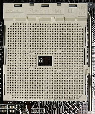
Socket FM1 is a CPU socket for desktop computers used by AMD early A-series APUs ("Llano") processors and Llano-derived Athlon II processors. It was released in July 2011. Its direct successors are Socket FM2 and Socket FM2+, while Socket AM1 is targeting low-power SoCs.
Socket FM2 is a CPU socket used by AMD's desktop Trinity and Richland APUs to connect to the motherboard as well as Athlon X2 and Athlon X4 processors based on them. FM2 was launched on September 27, 2012. Motherboards which feature the at the time new FM2 CPU socket also utilize AMD's at the time new A85X chipset.
Graphics Core Next (GCN) is the codename for a series of microarchitectures and an instruction set architecture that were developed by AMD for its GPUs as the successor to its TeraScale microarchitecture. The first product featuring GCN was launched on January 9, 2012.
Heterogeneous System Architecture (HSA) is a cross-vendor set of specifications that allow for the integration of central processing units and graphics processors on the same bus, with shared memory and tasks. The HSA is being developed by the HSA Foundation, which includes AMD and ARM. The platform's stated aim is to reduce communication latency between CPUs, GPUs and other compute devices, and make these various devices more compatible from a programmer's perspective, relieving the programmer of the task of planning the moving of data between devices' disjoint memories.
AMD Steamroller Family 15h is a microarchitecture developed by AMD for AMD APUs, which succeeded Piledriver in the beginning of 2014 as the third-generation Bulldozer-based microarchitecture. Steamroller APUs continue to use two-core modules as their predecessors, while aiming at achieving greater levels of parallelism.
AMD Excavator Family 15h is a microarchitecture developed by AMD to succeed Steamroller Family 15h for use in AMD APU processors and normal CPUs. On October 12, 2011, AMD revealed Excavator to be the code name for the fourth-generation Bulldozer-derived core.
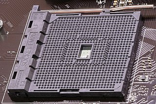
Socket FM2+ is a zero insertion force CPU socket designed by AMD for their desktop "Kaveri" APUs (Steamroller-based) and Godavari APUs (Steamroller-based) to connect to the motherboard. The FM2+ has a slightly different pin configuration to Socket FM2 with two additional pin sockets. Socket FM2+ APUs are not compatible with Socket FM2 motherboards due to the aforementioned additional pins. However, socket FM2 APUs such as "Richland" and "Trinity" are compatible with the FM2+ socket.
AMD's Socket FT3 or BGA-769 targets mobile devices and was designed for APUs codenamed Kabini and Temash, Beema and Mullins.
The Socket FT1 or BGA413 is a CPU socket released in January 2011 from AMD for its APUs codenamed Desna, Ontario, Zacate and Hondo. The uber name is "Brazos".
The Socket FP2 or μBGA-827 is a CPU socket for notebooks that was released in May 2012 by AMD with its APU processors codenamed Trinity and Richland.
The Socket FP3 or μBGA906 is a CPU socket for laptops that was released in June 2014 by AMD with its mobility APU products codenamed Kaveri.
AMD PowerTune is a series of dynamic frequency scaling technologies built into some AMD GPUs and APUs that allow the clock speed of the processor to be dynamically changed by software. This allows the processor to meet the instantaneous performance needs of the operation being performed, while minimizing power draw, heat generation and noise avoidance. AMD PowerTune aims to solve thermal design power and performance constraints.
Zen is the codename for the first iteration in a family of computer processor microarchitectures of the same name from AMD. It was first used with their Ryzen series of CPUs in February 2017. The first Zen-based preview system was demonstrated at E3 2016, and first substantially detailed at an event hosted a block away from the Intel Developer Forum 2016. The first Zen-based CPUs, codenamed "Summit Ridge", reached the market in early March 2017, Zen-derived Epyc server processors launched in June 2017 and Zen-based APUs arrived in November 2017.
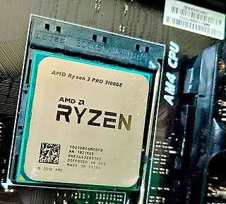
Ryzen is a brand of multi-core x86-64 microprocessors designed and marketed by AMD for desktop, mobile, server, and embedded platforms based on the Zen microarchitecture. It consists of central processing units (CPUs) marketed for mainstream, enthusiast, server, and workstation segments and accelerated processing units (APUs) marketed for mainstream and entry-level segments and embedded systems applications.
Zen+ is the codename for a computer processor microarchitecture by AMD. It is the successor to the first gen Zen microarchitecture, first released in April 2018, powering the second generation of Ryzen processors, known as Ryzen 2000 for mainstream desktop systems, Threadripper 2000 for high-end desktop setups and Ryzen 3000G for accelerated processing units (APUs).
The Radeon RX Vega series is a series of graphics processors developed by AMD. These GPUs use the Graphics Core Next (GCN) 5th generation architecture, codenamed Vega, and are manufactured on 14 nm FinFET technology, developed by Samsung Electronics and licensed to GlobalFoundries. The series consists of desktop graphics cards and APUs aimed at desktops, mobile devices, and embedded applications.
{{cite web}}
: CS1 maint: url-status (link)